
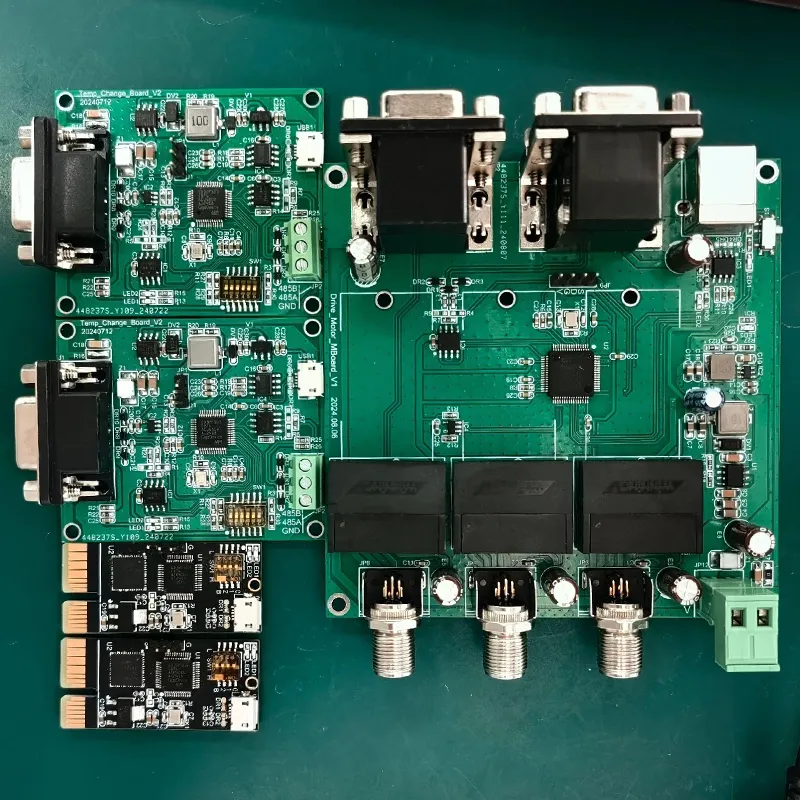
What is star grounding in PCB design?
When designing printed circuit boards (PCBs), grounding is critical. A common approach is star grounding. But what exactly is star grounding? Why is it crucial for your PCB design? Let’s break it down.
When designing printed circuit boards (PCBs), grounding is critical. A common approach is star grounding. But what exactly is star grounding? Why is it crucial for your PCB design? Let’s break it down.
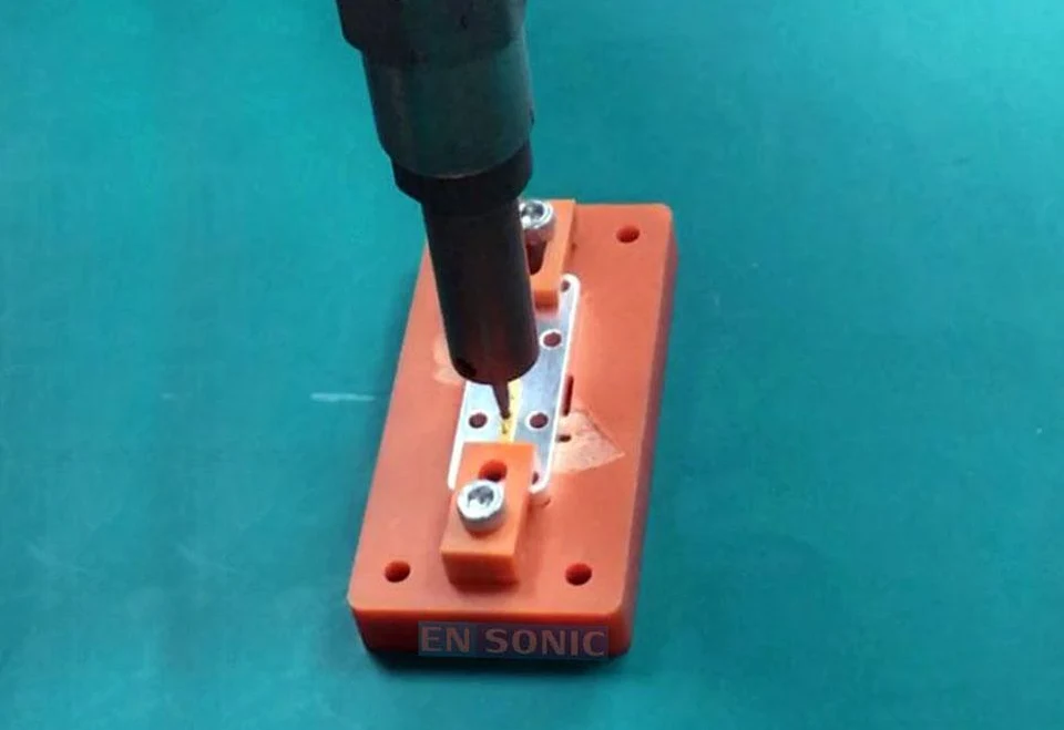
The miniaturization of microwave equipment has driven the development of microwave circuits toward smaller sizes, high integration, high reliability, low power consumption, and mass production.
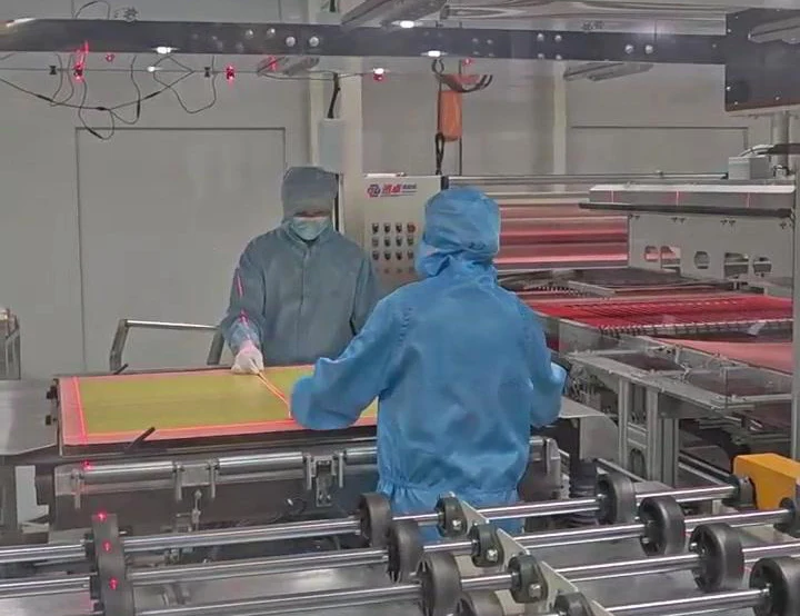
In recent years, with the development of electronic components and electronic assembly technologies, the line widths in new project designs have mostly been 0.1, 0.11, and 0.13 mm.
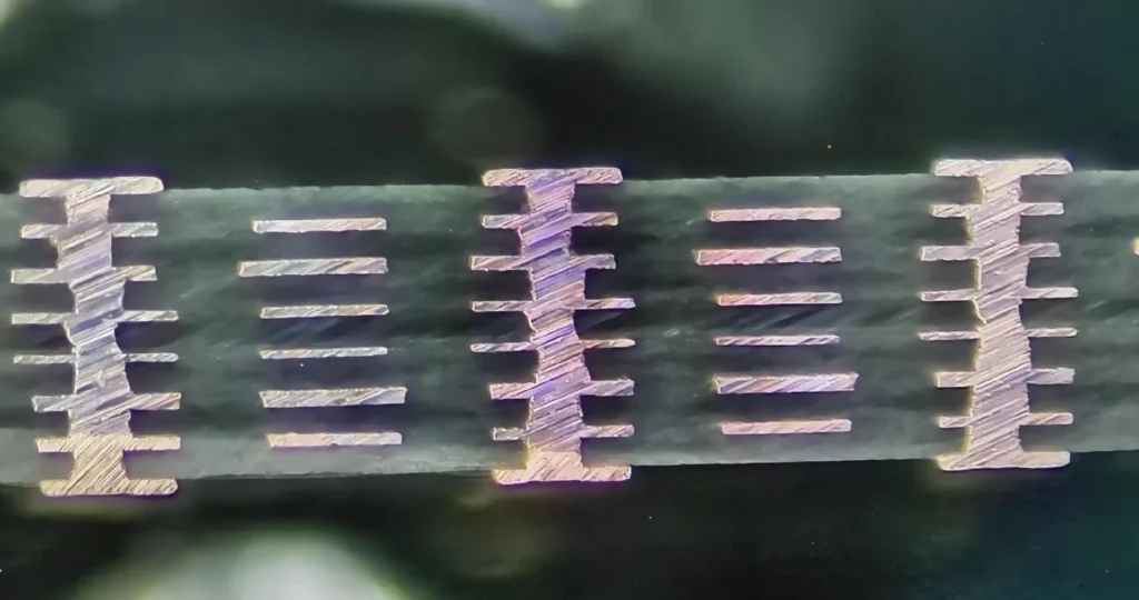
A PCB stackup refers to the arrangement of copper layers and insulating layers that make up a PCB prior to the layout design.
A while back, my TV wouldn’t turn on, so I had a repair technician replace the motherboard. I kept the old one.
This study focuses on finished chips that have already been packaged. Since there is no accurate model of their internal structure, the analysis primarily relies on external geometry and the layout of solder joints.
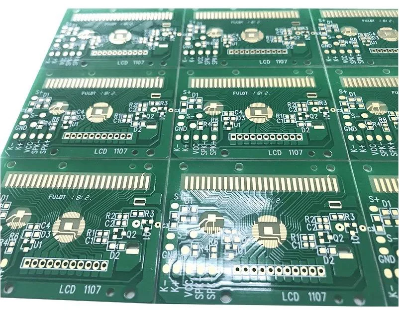
Vias are one of the key components of multilayer PCBs, and the cost of drilling typically accounts for 30% to 40% of the total PCB manufacturing cost.
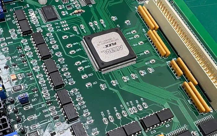
The electronics industry is rapidly evolving toward higher density and miniaturization. As the core structural component of various electronic devices, printed circuit boards (PCBs) are increasingly adopting multilayer designs, leading to ever-stricter requirements for forming precision.
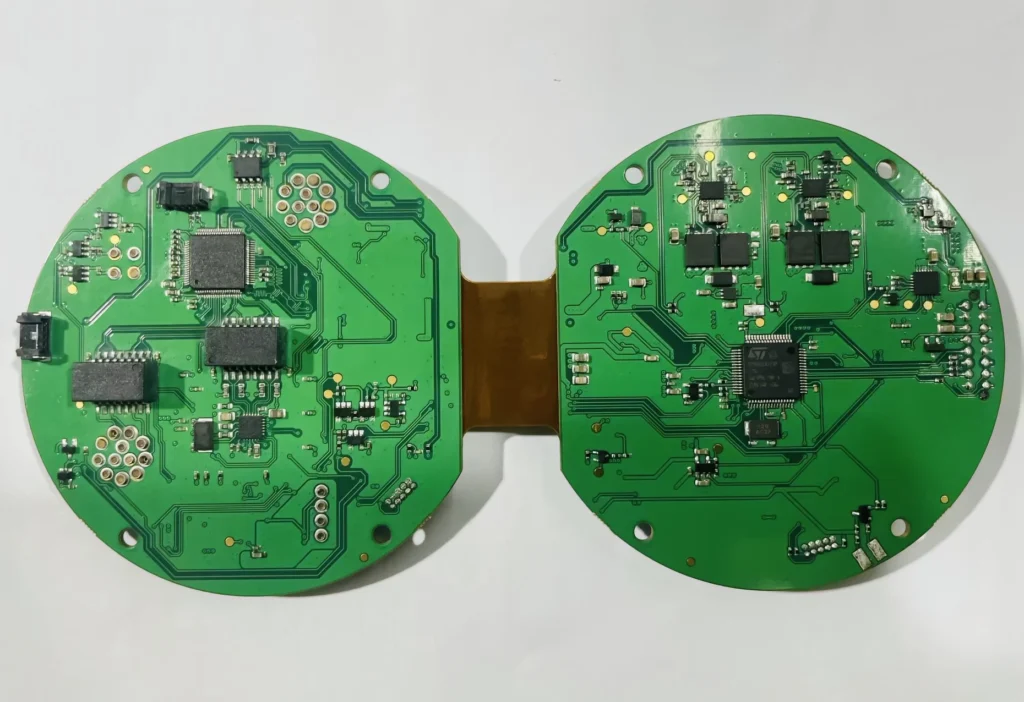
Specialized printed circuit boards (PCBs)—which incorporate embedded capacitors, resistors, and embedded or embedded metal blocks—enhance the functionality and scope of application of PCBs and offer high added value.
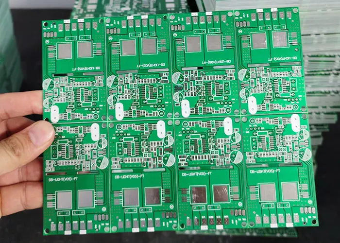
Discover how PCB copper thickness affects electrical conductivity, heat dissipation, and structural strength. Learn how to balance performance and cost in PCB design.