Specialized printed circuit boards (PCBs)—which incorporate embedded capacitors, resistors, and embedded or embedded metal blocks—enhance the functionality and scope of application of PCBs and offer high added value.
However, the fabrication of specialized PCBs is relatively challenging, and their manufacturing processes differ significantly from those of standard PCBs.
This paper presents a manufacturing method for a 4-layer, second-order embedded-core high-density interconnect (HDI) special-purpose PCB.
Analysis of Manufacturing Challenges
Layer Stackup
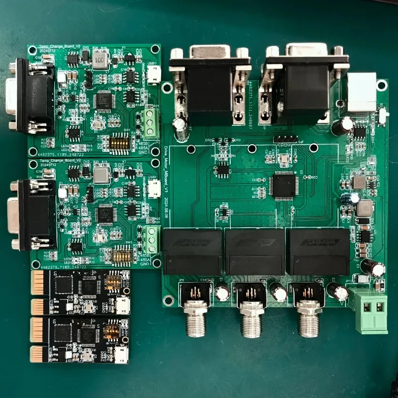
The structure of a 4-layer, second-order chip-embedded HDI board is shown in Figure 1.

Analysis of Manufacturing Challenges
(1) Lamination Challenges in Asymmetric PCB Structures
As shown in Figure 1, this PCB features an asymmetrical structure with two sets of single-sided blind vias.
The manufacturing process requires two lamination steps: the first lamination embeds the chip within the L3–L4 layers of the core board and bonds it to the L2 layer, completing the L2–L4 lamination;
Subsequently, blind vias between L2 and L3 and the L2 layer traces are fabricated, followed by a second lamination to bond the L1 and L2 layers.
Due to the asymmetric laminate structure, the finished PCB is prone to excessive warpage.
Optimizing the lamination structure to ensure good bending resistance is one of the key control points for this PCB (bending must be controlled within 0.65–1.52 mm).
(2) Laser Drilling and Plating for Oversized Blind Vias in HDI PCBs
This PCB design features laser-drilled blind vias with a dielectric layer thickness of 0.172 mm and a via diameter of 0.2 mm, both of which are significantly larger than the typical HDI specifications of 0.075 mm for dielectric layer thickness and 0.1 mm for via diameter.
Therefore, a high-energy laser drilling machine must be selected for laser processing of the blind vias.
Additionally, a dedicated plating process must be developed for the blind via plating and filling.
(3) Ensuring Void-Free Resin and Chemical Protection for L4-Exposed Chips
Since the chip is exposed on the L4 side, it must undergo chemical treatment processes such as electroless copper plating, electroplating, or immersion in leveling solutions during manufacturing.
If resin filling between the chip and the substrate is insufficient during lamination, resulting in gaps or voids, the chemical solutions may seep into these gaps and cause corrosion of the chip.
Avoiding residual voids or bubbles during lamination is a critical issue in this process.
This structure requires strict control over resin flow during lamination and the resin filling effectiveness between the chip and the substrate after lamination to ensure 100% void-free results.
(4) Pre-Lamination Chip Surface Treatment and Baking
Structurally, one side of the chip is bonded to the 1080 prepreg (PP) layers L2–L3.
Therefore, surface treatment of the chip prior to the first lamination is critical for enhancing bond strength.
Before lamination, the chip must undergo a browning treatment to increase surface roughness.
Due to the small size of the chip, the fan in the browning and drying section must be turned off to prevent the chip from being blown away by hot air.
After browning, the chip must be statically baked in an oven to remove moisture, with baking conditions set at 120 °C for 1 hour.
(5) Matching Thermal Expansion for PCB and Ceramic Chip
The packaging material for this chip is ceramic, which has a low coefficient of thermal expansion.
Since the chip is embedded within the PCB, the thermal expansion coefficients of the PCB material and the chip must be closely matched to ensure compatibility.
Therefore, selecting the appropriate PCB material is one of the key design considerations for this board.
Selection of PCB Structural Materials
An analysis of the manufacturing challenges reveals that when selecting materials for this board, factors such as improving board warpage, resin filling, and coefficient of thermal expansion must be taken into account.
Research on material selection for warpage control in asymmetric-structure boards indicates that the thinner the glass fiber cloth used in the PP laminate, the more effective it is in reducing warpage in asymmetric-structure boards.
For this board, both the laminated PP and the core board require the use of thin glass-fiber-reinforced PP.
The 0.2 mm core board must be laminated using 3 layers of 313×2 PP, with the laminate consisting of 1080 PP (high resin content, 68%).
Additionally, selecting materials with a low coefficient of thermal expansion and high Tg provides better dimensional stability (select boards with Tg ≥ 190 °C).
Tailored Manufacturing Process
Core Board Fabrication
As shown in Figure 1, there are four core boards: 1, 2, 3, and 4.
Core board 1 features only the L3 layer circuit; the opposite side is copper-free, and pilot holes are punched after etching.
The second and third boards have no circuits, and pilot holes are punched.
Core board 4 features a full copper L4 layer circuit; the opposite side is bare, and pilot holes are punched after etching.
Milling Grooves in Core Boards and PP
Select a CNC milling machine with a milling accuracy of ±0.050 mm to mill grooves that are 0.075 mm wider on each side than the chip; use the same method to mill grooves in the PP that are 0.125 mm wider on each side than the chip.
It is recommended to install the CNC milling machine in a lamination cleanroom, as PP must be stored in an environment with stable temperature and humidity and meeting cleanliness standards to ensure high-quality lamination.
First Lamination
After the first lamination is complete, the PCB thickness ranges from 1.35 to 1.65 mm.
(1) Chromate Treatment and Baking of PCB Chips
Perform standard chromate treatment on the core boards (1, 2, 3, 4); chips must be treated using a carrier.
Take special care to turn off the blower during the drying stage.
After chromate treatment, bake in an oven at 120°C for 1 hour.
(2) Ensuring Chip Alignment During Lamination
To prevent chip misalignment caused by core board slippage during lamination, the core board alignment deviation must be within 0.075 mm.
Use pinning lamination (PIN LAM) for positioning; if PIN LAM equipment is unavailable, secure the core board with 12 rivets and fuse them using an electromagnetic hot-melt machine after riveting.
(3) Layer Stacking and Chip Placement Procedure
When stacking the layers, first place the adhesive-resistant film on the steel plate: if using a PIN LAM press, the adhesive-resistant film must be pre-punched, and the PP must also be pre-punched; if using rivets and fusion for positioning, place the core board with completed rivets and fusion onto the adhesive-resistant film.
Wear adhesive-resistant gloves to place the chip into the slot, stack the 1080×2 PP between L2 and L3, cover with the L2 copper foil layer, and finally cover with the steel plate, for a total of 10 layers.
(4) Critical Lamination Parameter Settings
The setting of lamination parameters is critical. After high-temperature curing during lamination, the pressure during the cooling phase should be set to 10 kg/cm² or lower to allow the PCB to cool slowly under low pressure; another key point is to ensure sufficient resin fills the gaps around the chip, so select 1080 PP with a resin content of 68%.
During the lamination process, when the material temperature is in the 80–120 °C range, the heating rate should be increased (3.5 °C/min; the higher the heating rate, the better the resin flow and filling properties), and a higher peak pressure (32 kg/cm²) should be set.
Post-Processing After the First Lamination
After the first lamination, the specific processing steps are as follows:
(1) Trim the board edges and drill alignment holes.
Use an X-ray drilling machine to drill the PCB’s alignment holes, and process the board edges using a trimming line.
(2) Remove residual resin from the chip surface.
Use laser processing to remove residual resin from the chip surface, ensuring a fill rate of 90%.
(3) Remove resin residue from the board surface.
Send the board to the electroplating process for a resin removal step to eliminate residual resin from the PCB copper surface.
(4) Inspect the chip flatness using a 3D measuring instrument. The flatness of the chip relative to the board surface must be within −10 to +20 μm.
L2 Laser Drilling of Blind Holes
Specific steps for L2 laser drilling of blind holes:
(1) Drill pilot holes, expose them using a specialized photoresist, etch the board with an acidic solution, and etch out the window areas for the blind holes.
(2) Laser drilling of blind holes is performed on the L2 side with a hole diameter of 0.2 mm, using a Mitsubishi laser drilling machine.
L2 Blind Hole Plating
The specific steps for L2 blind hole plating are as follows:
(1) After laser drilling, perform plasma desmearing to remove residual adhesive from the blind holes.
(2) Run the blind holes through a cleaning machine (with the brush section disabled) for chemical cleaning; ensure the water pressure is set within the upper limit range.
(3) Use a dedicated automated optical inspection (AOI) machine to inspect the bottoms of the L2 blind vias and confirm that there is no resin residue inside the holes.
(4) Bake the board at 200 °C for 2 hours prior to electroless copper plating, then complete the electroless copper plating on the horizontal plating line.
L2 Via-Filling Electroplating
The specific steps for L2 via-filling electroplating are as follows:
(1) During the first blind via electroplating process, no current is applied to the non-blind via side.
The minimum copper thickness for blind vias is 15 μm, and the overall board copper thickness is 75–95 μm.
(2) Prepare the dry film for plating.
This is done after the outer layer circuit process is completed, leaving the blind holes exposed while covering the entire non-blind hole surface with the film.
(3) During the second plating cycle, only the holes are plated, not the board surface, to ensure 100% filling of the blind holes.
(4) Film stripping: Remove the dry film from the board surface on the stripping line.
(5) During board grinding, activate only the L2 side grinding brushes; do not activate the L4 side.
After grinding, the copper thickness on the back side should be controlled between 65 and 85 μm, with copper fill recesses ≤20 μm and protrusions ≤25 μm.
(6) After grinding is complete, proceed with surface plating.
The minimum copper thickness on the L2 front side should be controlled at 105 μm; no current is applied to the L4 side.
L2 Layer Circuit Fabrication
The specific steps for L2 layer circuit fabrication are as follows:
(1) For the L2 layer, a photoresist dry film is used, and the pattern is transferred via laser direct imaging (LDI).
For the L4 layer, a resist dry film is applied and fully exposed.
(2) Etching is performed on the acid etching line; the L2 layer is etched to form the circuit patterns, while the L4 layer is masked.
After etching, a stripping process is performed.
(3) The L2 layer circuit patterns are inspected on an AOI machine.
Second Lamination
The specific steps for the second lamination are as follows:
(1) Pre-bake the board at 120°C for 2 hours before browning, and pre-bake it again at 120°C for 2 hours after browning.
(2) Pre-stack the board, placing 1080×2 PP on layers L1–L2.
(3) Before stacking, place copper foil (with the rough side facing the steel plate) or release film on the steel plate.
Then place the pre-stacked boards with the L4 side facing down, and place 17 μm copper foil on top of the 1080×2 PP on layers L1–L2.
(4) Control the lamination parameters; set the lamination pressure during the cooling phase to 10 kg/cm² or less to allow the PCB to cool slowly under low pressure, thereby reducing internal stress caused by lamination.
Post-Processing After the Second Lamination
After the second lamination, the specific processing steps are as follows:
(1) After lamination, use an X-ray machine to drill positioning holes, followed by rounding and edge grinding on the cutting and grinding line.
(2) Send the PCB to the electroplating process for the resin removal step to remove any residual resin from the copper surface of the board.
L1 Copper Reduction
The steps for L1 copper reduction are as follows:
(1) Prepare the outer layer dry film; do not cover the L1 layer, but cover the L4 layer.
(2) Reduce the copper thickness of the L1 layer to 7–9 μm along the copper reduction lines.
(3) Perform a stripping process to remove all the dry film covering the L4 layer.
L1 Laser Drilling
The processing steps for L1 laser drilling are as follows:
(1) Expose the blind via positions on the L1 side using a photoresist to create openings; fully expose the L4 side to create a resist mask.
Etch the board with an over-acid solution to etch out the blind via positioning openings on the L1 side; then perform a stripping process.
(2) Laser drilling of blind vias: Drill from the L1 side with a hole diameter of 0.2 mm using a Mitsubishi laser drilling machine.
L1 Blind Via Plating
The process steps for L1 blind via plating are as follows:
(1) After laser drilling, perform plasma desmearing.
(2) Chemically clean the blind vias in a cleaning machine; disable the brush section before cleaning.
(3) Inspect the L1 blind vias using a dedicated AOI inspection machine, focusing on checking for resin residue at the bottom of the blind vias.
(4) Bake the board at 200°C for 2 hours prior to chemical copper plating, then process the board on the horizontal copper plating line.
L1 Via-Filling Electroplating
The processing steps for L1 via-filling electroplating are as follows:
(1) Maintain a minimum copper thickness of 15 μm for blind vias and 50–70 μm on the board surface during the first via-filling electroplating, keeping the L4 side unenergized.
(2) After the first hole-filling electroplating, apply a dry film to the L1 side, leaving the blind hole positions exposed, and cover the entire L4 side with dry film.
(3) Plate only the holes during the second hole-filling electroplating, keeping the L4 side unenergized.
(4) Remove the dry film from the board surface on the stripping line.
(5) During board grinding, activate the grinding brushes only on the L1 side; do not activate them on the L4 side.
Control the copper thickness between 40 and 60 μm after grinding, keeping the copper in the plated holes with a depression of ≤20 μm and a protrusion of ≤25 μm.
Through-Hole Fabrication
The steps for through-hole fabrication are as follows:
(1) Send the board to the mechanical drilling process to create through-holes.
(2) Chemical copper plating of through-holes: Before plating, bake the board at 200 °C for 2 hours, then complete the standard copper plating process.
(3) Surface plating: After sanding the board, perform surface plating. Apply L1 plating; do not apply current to the L4 surface.
Outer Layer Circuit Fabrication
The fabrication process for outer layer circuits is as follows:
(1) Manufactured using specialized circuit materials, photoresist dry film, and an LDI exposure system.
(2) Etched on an acid etching line; the L1 layer retains the circuit patterns, while the L4 layer has no circuit patterns.
(3) Inspect the outer layer circuits using an AOI machine.
Solder Mask Application and Subsequent Processes
The solder mask application and subsequent processes are as follows:
(1) Apply the solder mask following standard procedures: use a volcanic ash grinding board, perform screen printing, low-temperature baking, exposure, development, and high-temperature baking; leave the chip areas on Layer 4 copper-exposed, and fully cover all other areas with solder mask.
(2) The surface treatment method for this board is electroless gold plating, using standard procedures.
(3) Complete forming using a CNC milling machine.
(4) When performing open-circuit and short-circuit testing, ensure that the chip can withstand a voltage of ≥1,000 V.
(5) Cure the board in a dedicated board bending and curing oven at 150 °C for 4 hours, then perform 100% testing on a board bending tester (control board bending within 0.65 mm/1.52 mm).
(6) Finally, perform a surface quality inspection using an automated visual inspection (AVI) machine to check the PCB’s appearance; after the quality control department confirms compliance through random sampling, proceed with packaging and shipment.
Quality Analysis of Key Process Items
Panel Warpage Data
Sampled warpage data from 50 finished units after completing the panel bending process.
The requirement was for panel warpage to be within 0.65 mm/1.52 mm; the actual measurements were 0.53–0.63 mm/1.41–1.51 mm, which met the requirements.
The measurement data indicates that although the panel structure is asymmetrical, by optimizing panel selection, adjusting lamination parameters, and establishing a panel bending process prior to final inspection, we ensured that 100% of the panel bending data fell within the customer’s acceptable standards.
Chip Flatness Data
After lamination, the chip flatness tolerance range is −10 to +20 μm (concave/convex).
Sampled 50 chip locations after removing the adhesive residue and measured concave/convex values of −1.0 to −8.0 μm.
Following this lamination process, all chip flatness data fall within the specified tolerance range and are negative values.
Microscopic Examination of Voids
Sectioned 20 chips after lamination to examine voids between the chips and the substrate.
Observed no voids in any of the 20 sections.
This indicates that the use of 1080 PP with a high resin content during lamination, combined with slot milling of the core board using a high-precision CNC milling machine—with slot widths controlled to within 0.075 μm on each side—ensured effective resin filling.
Reliability of Reflow Soldering
Passed five finished products through the reflow oven three times at 270°C and performed cross-sectional analysis to check for delamination between the chip and the substrate.
Confirmed no delamination between the chip and the substrate and found no fractures at the chip-to-blind-via connections.
Conclusion
Conducted an in-depth study on this 4-layer, second-order embedded chip PCB and developed corresponding control measures to address various issues.
Through process testing and validation, data on board warpage, chip flatness, and reflow soldering reliability all fell within the customer’s acceptable standards, confirming the quality feasibility of the manufacturing plan.
However, the manufacturing process is relatively complex, involving 51 steps, and requires further optimization.