When it comes to electronic devices, one cannot overlook the PCB (printed circuit board)—this core component acts as the device”s “nerve center,” coordinating the smooth operation of all its functions.
Yet few people realize that the performance of a PCB is closely tied to a seemingly minor detail: the thickness of its copper layer.
Today, we’ll demystify the importance of copper thickness and explore how it quietly determines the quality and lifespan of the electronic devices in your hands.
Conductive Core: Ensuring Unimpeded Current Flow
Copper is an indispensable conductive material in PCBs, and the thickness of the copper layer directly determines electrical conductivity.
A thicker copper layer provides a wider “current pathway,” allowing electrons to flow more smoothly.
This not only stabilizes circuit voltage but also reduces signal interference and loss.
Conversely, if the copper layer is too thin, it’s like navigating a narrow alley—current is prone to “congestion.”
At best, this causes devices to respond slowly; at worst, it leads to circuit short-circuits, data loss, and other malfunctions.
| Interposer | Substrate |
|---|---|
| Located between the chip and the package substrate, or between multiple chips in 2.5D/3D packaging | Forms the foundational layer of the package, used to connect with the PCB |
| Its primary function is to redistribute signals and manage fine-pitch interconnections that cannot be directly routed | Typically made of organic laminate materials (such as BT resin, ABF film); ceramics are used in some high-reliability applications |
| Can be made of silicon, glass, or organic materials | Has much larger connection pitch compared to interposers — connects the package to the PCB through solder balls (BGA) |
| For vertical interconnection, it usually includes TSV (Through-Silicon Via) | Functionally more like a “mini PCB” |
| Features ultra-fine pitch — capable of supporting micrometer-scale line widths | Relatively low cost and suitable for mass production |
| More complex structure and higher cost (especially silicon interposers); mainly used in high-performance computing applications (HPC, GPU, FPGA, HBM integration, etc.) | Standard structure in almost all semiconductor packages (e.g., CPU, smartphone chips, memory chips, etc.) |
Table 1. Comparison Between Interposer and Substrate
Key to Heat Dissipation: “Cooling Down and Reducing the Load” on Devices
As electronic devices evolve toward higher power and smaller sizes, heat dissipation has become an increasingly critical issue.
Copper inherently possesses excellent thermal conductivity, and the thickness of the copper layer serves as a “barometer” of heat dissipation capability.
When a device is in operation, the heat generated by components is transferred to the copper layer.
Role of Copper Thickness in Thermal Distribution
A thicker copper layer can rapidly distribute this heat across the entire circuit board, which is then expelled through the heat dissipation structure.
If the copper layer is too thin, heat will accumulate in localized areas—much like a stuffy room without ventilation.
This not only causes the device to lag or throttle its performance but also accelerates component aging due to prolonged high temperatures, thereby shortening the device’s lifespan.
It’s similar to a cast-iron skillet used for stir-frying: the thicker the bottom, the more evenly the heat is distributed, making it less likely for food to burn in specific spots.
Evolution of Interposer Technologies
| Generation | Timeframe & Type | Key Examples | Description / Features |
|---|---|---|---|
| 1st Generation: Passive Interposer | Early 2000s – Early 2010s | Xilinx Virtex-7 2000T FPGA (2011) | First commercial product using TSV-based passive silicon interposer; supports integration of multiple FPGA dies on a single interposer |
| TSMC CoWoS (introduced ~2012) | Enables chip–wafer–substrate integration (CoWoS) for GPU/ASIC; first widely adopted passive interposer platform for GPUs and network processors | ||
| NVIDIA GPUs with HBM (Pascal/Volta) | Uses silicon interposers to place HBM stacks alongside GPU dies | ||
| 2nd Generation: Organic & Glass Interposers | Mid-2010s | Organic interposers in networking ASICs and FPGAs | Provided by ASE, Ibiden, etc. for networking processors (e.g., Broadcom, Cisco) using organic laminate substrates |
| Glass interposer R&D (Corning, Schott, Georgia Tech) | Demonstrated low-loss and stable CTE glass substrates; early prototypes focused on RF and high-speed networking | ||
| JEDEC exploration for HBM | Investigating glass as a lower-cost alternative for memory interposers | ||
| 3rd Generation: Bridge & RDL Fan-Out Technologies | Late 2010s – Early 2020s | Intel EMIB (since 2017) | Embedded Multi-die Interconnect Bridge; first used in Kaby Lake-G (Intel CPU + AMD Radeon GPU + HBM), later in Stratix 10 FPGA and Ponte Vecchio GPU |
| TSMC InFO (Integrated Fan-Out) | Widely used in Apple A-series SoCs (from A10/A11); TSV-free RDL interposer layer for IO redistribution | ||
| Samsung eWLB | Embedded wafer-level ball grid array packaging; enables multi-chip integration via fan-out redistribution | ||
| 4th Generation: Active Interposer | 2020s – Future | Cerebras Wafer-Scale Engine (2019–present) | Not a traditional interposer; integrates compute cores and power delivery network into a single active interposer-like wafer |
| TSMC system-level integration chips | Roadmaps include active interposers with integrated chiplet control | ||
| CEA-Leti / Imec prototypes | Demonstrations of active interposers with embedded regulators, clock trees, and optical interconnects | ||
| Intel Foveros Direct (3D stacking with active base die) | Functions similarly to an active interposer, integrating interconnect and power management in the base die |
Table 2. Development of Interposers
Structural Support: Making PCBs “Indestructible”
In addition to conducting electricity and dissipating heat, copper thickness directly affects the physical strength of a PCB.
A thicker copper layer enhances the board’s toughness, making it more resistant to damage caused by bending and vibration during assembly, transportation, or daily use, thereby reducing the risk of breakage.
At the same time, thicker copper layers provide a larger soldering area for component leads, resulting in more secure solder joints and reducing failures caused by poor contact.
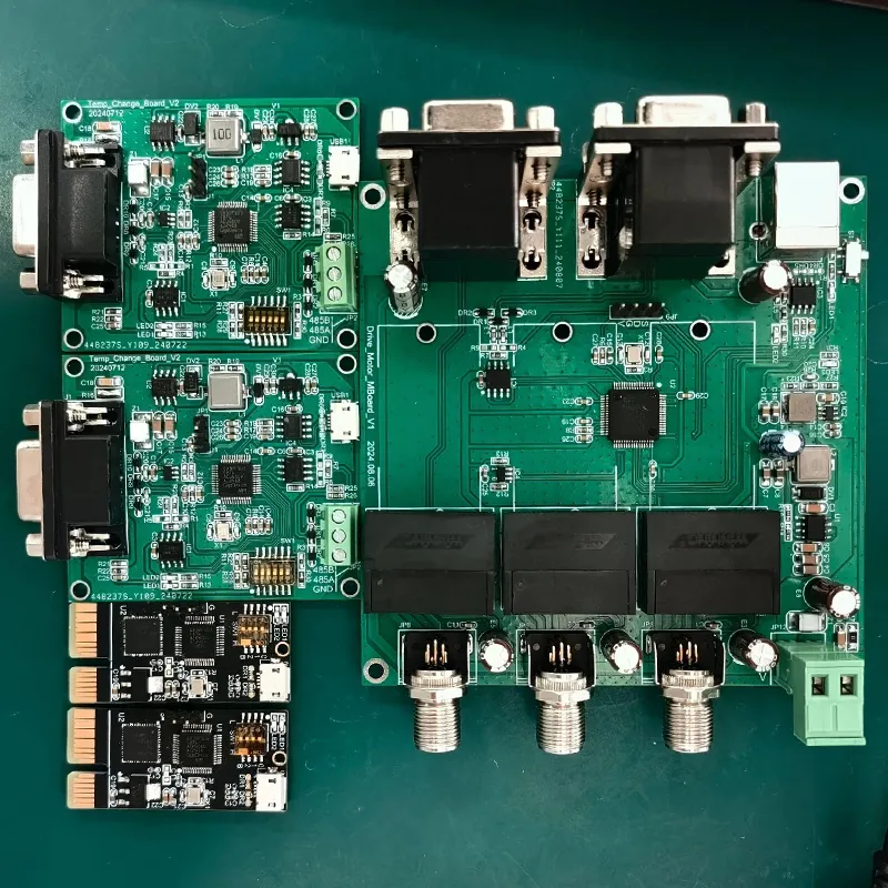
Simply put, thick copper layers act like a “reinforcing skeleton” for the PCB, making it more durable and extending its service life.
Figure 3
The Art of Balance: Finding the “Optimal Solution” Between Cost and Performance
However, thicker is not always better when it comes to copper layers.
The cost of copper accounts for a significant portion of PCB manufacturing expenses; excessively thick copper layers can substantially increase production costs, which ultimately are reflected in the product’s retail price.
Therefore, PCB manufacturers must precisely control copper thickness based on the product’s actual requirements:
for example, products with extremely high stability requirements, such as industrial equipment and servers, will use thicker copper layers;
whereas small consumer electronics, such as smart bracelets and headphones, will opt for more economical copper thicknesses while ensuring basic performance.
This is akin to putting together an outfit—one must meet the demands of the occasion while staying within budget, finding the most suitable “balance point.”
Figure 4
Copper Thickness: The “Health Code” of Electronic Products
From electrical conductivity to heat dissipation, and from structural strength to operational costs, copper thickness acts as an invisible thread running through the very core of a PCB’s performance.
Choosing the right copper thickness not only ensures that electronic products operate stably and smoothly but also extends their service life, sparing users the hassle of frequent repairs.
The next time you use your smartphone, computer, or other devices, take a moment to think about the layer of copper hidden inside—it is this “invisible guardian” that quietly provides reliable support for every action you take.
Conclusion
Copper thickness plays a critical role in defining the performance, durability, and reliability of electronic devices. It directly influences electrical conductivity, heat dissipation, and structural strength, serving as the backbone that supports stable device operation.
While thicker copper layers enhance current flow, dissipate heat more efficiently, and strengthen the PCB against bending and vibration, excessive thickness increases manufacturing costs.
Achieving the right balance between performance and cost is essential, as the optimal copper thickness ensures devices function smoothly, last longer, and maintain reliability without unnecessary expense.
In essence, copper thickness acts as the “invisible guardian” of electronic products, quietly sustaining their efficiency and longevity.