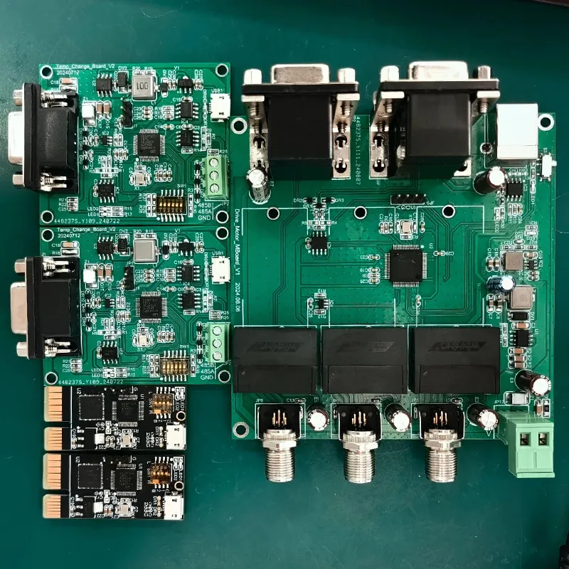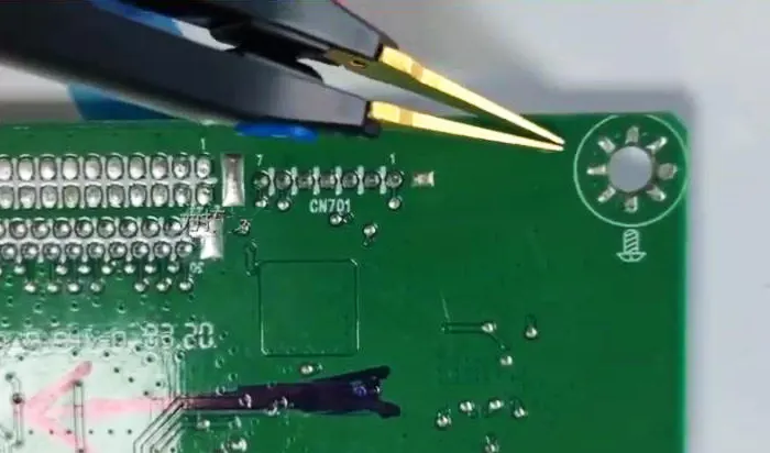
In recent years, with the development of electronic components and electronic assembly technologies, the line widths in new project designs have mostly been 0.1, 0.11, and 0.13 mm.
However, for printed circuit boards with line widths ranging from 0.1 mm to 0.15 mm, outsourcing the entire board has led to increased outsourcing costs.
To address the manufacturing challenges of PCBs with line widths ranging from 0.1 mm to 0.15 mm, process research on the outer layer etching of fine lines is necessary to resolve these bottlenecks.
Based on this, this paper introduces a production process for the outer layer etching of fine lines.
By improving the stripping solution, refining the etching process route, optimizing copper thickness, and controlling the etching solution concentration, the etched PCBs with a line width of 0.1 mm meet inspection requirements.
Technical Specifications
The printed circuit board meets the requirements of the “General Specifications for Rigid PCBs” (GJB 362C—2021). The key specifications are as follows:
(1) After etching, the side etch of the printed circuit board with a line width of 0.1 mm must be less than 20%.
(2) The etched PCB surface shall be free of residual copper foil, cracks, broken lines, and short circuits.
Pads shall be free of pinholes, flared holes, and elliptical holes.
When inspected using AOI equipment, notches or pinholes on the lines shall not exceed 20% of the original line width.
Selection of Prototypes and Materials
Selection of Prototypes
The core of the outer layer etching process for high-speed printed circuit boards (PCBs) lies in achieving a balance between high-precision circuit patterns and low-loss transmission performance.
The selection of prototypes must closely align with high-speed signal transmission requirements, with particular emphasis on the following factors:
(1) Transmission Rate Compatibility:
A 16-layer board designed for a transmission rate of no less than 10 Gbps is selected as the base prototype.
Its outer layer traces must carry high-frequency signals, imposing stringent requirements on etching depth and trace width consistency.
(2) Structural Complexity:
The prototype includes 0.2mm-diameter vias located in a dense routing area (with a minimum line width and spacing of 0.1mm) to simulate signal integrity challenges in real-world high-speed scenarios.
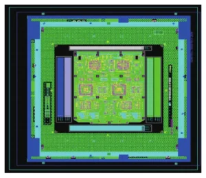
Therefore, the PCB with engineering file SYB1234 (see Figure 1) was selected, featuring a minimum line width of 0.1 mm, a line spacing of 0.1 mm, 16 layers, a layer thickness of 3.0 mm, and dimensions of 180 mm × 230.5 mm.
Material Selection
The selection of the substrate and copper foil directly affects etching accuracy and signal loss.
(1) Substrate Type:
A PTFE composite material with a low dielectric constant (Dk ≤ 3.5) and low loss factor (Df ≤ 0.005) is used.
Its chemical stability minimizes substrate damage during the etching process while meeting the low-latency requirements of high-frequency signals.
(2) Copper Foil Specifications:
Ultra-low profile (VLP) electrolytic copper foil with a surface roughness of Ra ≤ 0.5 μm is selected.
Compared to traditional copper foil, the smooth surface of VLP copper foil reduces etching side etch by more than 30% and improves the control of the skin effect in high-frequency signals.
(3) Thickness Adaptability:
The thickness of the outer layer copper foil must balance etching rate and current-carrying capacity to avoid uneven etching caused by excessively thick foil or signal attenuation caused by excessively thin foil.
| Copper Thickness (μm) | Single-Pass Etching Speed (m/min) | Double-Pass Etching Speed (m/min) | Line Width After Etching (mm) |
|---|---|---|---|
| 20 | 3.1 | 4.6 | 0.92 |
| 25 | 2.6 | 4.3 | 0.91 |
| 30 | 2.1 | 4.0 | 0.90 |
Table 1. Relationship between different etching methods and copper thickness for 0.1mm linewidth printed circuit boards.
Test Process and Results
Effect of Stripping Solution on Outer Layer Etching
Sodium hydroxide corrodes lead-tin alloys, leading to bright spots, tin dissolution, and film entrapment.
This issue is more prevalent on fine lines, resulting in high rework rates.
Therefore, following preliminary research on multiple stripping solution manufacturers, it was determined that currently available stripping solutions are not compatible with front-end stripping equipment used in etching processes;
Equipment modifications are required for their use. To avoid modifications, the production workshop collaborated with the manufacturer to develop an organic stripping solution specifically designed for the equipment.
This stripping solution offers advantages such as fast stripping speed, high solubility, and a long service life.
Optimal process parameters: concentration 10%–15%, conveying speed 1.1–1.3 m/min, and a control temperature of 50°C.
Figure 3 shows the results using sodium hydroxide stripping solution (with film adhesion and bright discs) prior to the improvement.
Figure 4 shows the results using the organic stripping solution (no film adhesion and bright discs) after the improvement.
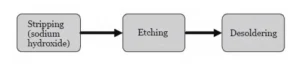
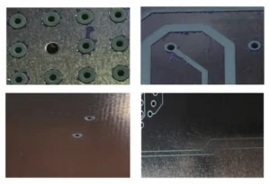
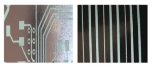
A comparison of Figures 3 and 4 highlights the performance difference between stripping methods.
An organic stripping solution eliminates bright spots during the stripping process.
The process removes film entrapment issues caused by fine lines and narrow line spacing.
Fine-line stripping stability improves as a result of these changes. These improvements support reliable etching of fine-line structures.
Effect of Etching Rate on the Outer Layer
Adjusting the etching speed is also a critical factor during the etching process.
For printed circuit boards with a copper thickness of 25 μm and a line width of 0.1 mm, a single etching pass results in significant side etching and narrowing of the lines.
Two-Pass Etching Method for Improved Line Control
The relationship between different etching methods and copper thickness for printed circuit boards with a 0.1 mm line width is shown in Table 1.
By performing two etching passes—that is, extending the etching segment length—for a copper thickness of 20 μm, the etching speed for a PCB with a 0.1 mm line width increased from 3.1 m/min in a single pass to 4.6 m/min in two passes, resulting in a post-etching line width of 0.92 μm.
For a PCB with a copper thickness of 25 μm and a line width of 0.1 mm, the etching speed increased from 2.6 m/min for a single pass to 4.3 m/min for two passes, with a post-etching line width of 0.91 μm.
For a printed circuit board with a copper thickness of 30 μm and a line width of 0.1 mm, the etching speed increased from 2.1 m/min for a single pass to 4.0 m/min for two passes, with a post-etching line width of 0.90 μm.
The experimental results indicate that the two-pass etching process effectively resolves the issue of insufficient etching capacity caused by the etching section being too short.
| Copper Thickness (μm) | Single-Pass Etching Speed (m/min) | Double-Pass Etching Speed (m/min) | Line Width After Etching (mm) |
|---|---|---|---|
| 20 | 3.1 | 4.6 | 0.92 |
| 25 | 2.6 | 4.3 | 0.91 |
| 30 | 2.1 | 4.0 | 0.90 |
Table 1. Relationship between different etching methods and copper thickness for 0.1mm linewidth printed circuit boards.
The Effect of Base Copper Thickness on Outer Layer Etching
As is well known, PCB traces are formed through chemical etching.
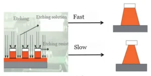
During etching, the etchant begins at the exposed copper surface and gradually etches inward; as it etches inward, it also etches horizontally into the adjacent copper foil.
The vertical and horizontal etching rates are constant and can be characterized by the etching factor.
During the etching process, the thicker the copper layer, the longer the vertical etching takes, and the greater the lateral etching, resulting in increased over-etching of the line width.
To verify the effect of board copper thickness on the line width during alkaline etching, experiments were conducted using H/T copper-clad laminates of different thicknesses (17μm/12μm), 1/H copper-clad laminates (35μm/12μm) with copper reduction, and 1/H copper-clad laminates (35μm/12μm).
After photolithography and electroplating, the copper thicknesses were 20, 25, and 30μm, respectively.
| Copper-Clad Laminate | Copper Thickness (μm) | Etching Rate (m/min) | Line Width After Etching (μm) |
|---|---|---|---|
| H/T (17μm / 12μm) | 20 | 4.6 | 0.92 |
| 1/H (35μm / 12μm) + Copper Filling | 25 | 4.3 | 0.91 |
| 1/H (35μm / 12μm) | 30 | 4.0 | 0.89 |
Table 2 Etching Results for Copper-Clad Laminates of Different Thicknesses
The Effect of Alkaline Etching Solution Concentration on Outer Layer Etching
The study uses the SYB1234 substrate as the test board to investigate the effect of alkaline etching solution concentration on the etching process.
The experiment optimizes the alkaline etching solution with copper ion concentrations ranging from 120 to 170 g/L and chloride ion concentrations ranging from 170 to 210 g/L.
The process performs etching under these varying conditions and collects line width data.
Table 3 presents the relationship between alkaline etching solution concentration and line width.
The etching process employed a controlled variable method, ensuring that the SYB1234 test board underwent two etching passes at a constant speed of 4.3 m/min.
Copper and chloride ion concentrations vary in tandem during the process.
The study evaluates copper ion concentrations of 120, 130, 140, 150, 160, and 170 g/L. The experiment processes selected boards through alkaline etching.
The system collects line width data during each test condition. Table 3 shows that a copper concentration of 150 g/L produces the best line width results.
When the process increases the concentration further, the line width decreases, and the solution tends to precipitate.
When the system maintains the copper ion concentration at 150 g/L, Cu(NH₃)₂Cl in the etching solution rapidly converts to Cu(NH₃)₄Cl₂, and the reaction increases the etching rate.
As the concentration increases, the copper and chloride ions in the solution increase its viscosity, slowing down the reaction of oxygen and hindering the reaction process, which in turn slows down the etching rate.
Therefore, controlling the copper ion concentration at 150 g/L during the etching process can effectively increase the reaction rate and reduce side etching.
| Cu (g/L) | Top Side 1 | Top Side 2 | Top Side 3 | Bottom Side 1 | Bottom Side 2 | Bottom Side 3 |
|---|---|---|---|---|---|---|
| 120 | 0.081 | 0.078 | 0.080 | 0.082 | 0.083 | 0.079 |
| 130 | 0.083 | 0.083 | 0.082 | 0.083 | 0.083 | 0.089 |
| 140 | 0.086 | 0.090 | 0.085 | 0.087 | 0.087 | 0.088 |
| 150 | 0.094 | 0.095 | 0.096 | 0.096 | 0.093 | 0.094 |
| 160 | 0.086 | 0.090 | 0.085 | 0.087 | 0.086 | 0.085 |
| 170 | 0.081 | 0.080 | 0.077 | 0.082 | 0.083 | 0.079 |
Table 3 Relationship Between Alkaline Etching Solution Concentration and Line Width
Conclusion
Evaluation and verification of etching behavior for printed circuit boards with 0.1 mm line widths define the basis for controlling outer layer etching performance.
Engineers replace sodium hydroxide stripping solution with an organic stripping solution. Manufacturing lines implement two etching passes to extend the etching segment length.
Production processes select H/T-thickness copper-clad laminates or reduce copper thickness to lower surface copper loading. Process control systems regulate copper ion concentration at 150 g/L.
These methods together ensure stable processing of printed circuit boards with 0.1 mm line widths.