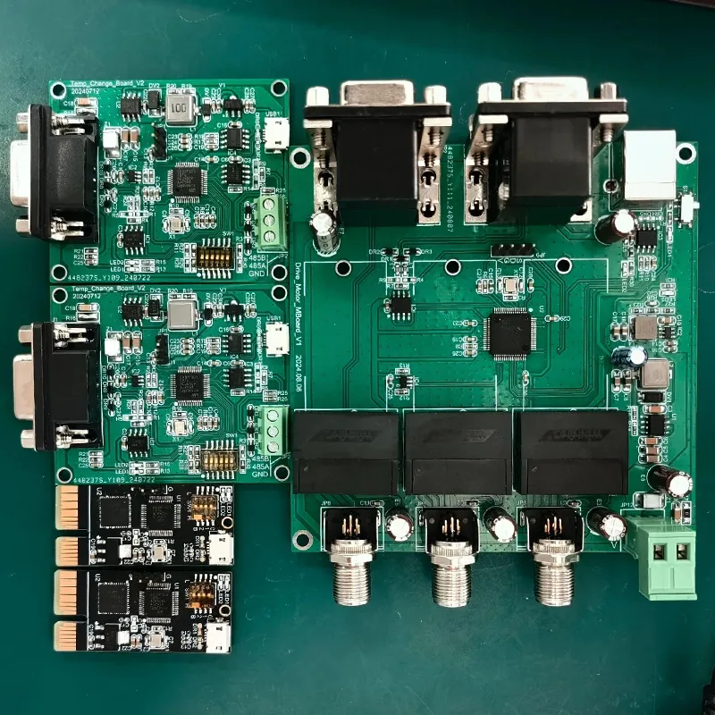
PCB layout is far more than just connecting components and passing DRC checks—it is the foundation of a product’s electromagnetic compatibility (EMC) performance.
Many beginner engineers focus on trace connectivity and visual neatness, overlooking how current flows, how noise couples, and where interference enters and propagates.
The truth is that EMC doesn’t start during post-production rectification;
it begins at the layout stage. Poor layout decisions can create oversized current loops, broken return paths, and misplaced noise sources—problems that become extremely costly and time-consuming to fix later.
This article presents 12 practical, field-proven PCB layout rules that help engineers avoid the vast majority of EMC issues right from the design phase.
When many beginners first start designing PCBs, they focus primarily on whether “the traces are connected,” “the DRC checks pass,” and “the board looks neat.”
While these factors are certainly important, from an EMC perspective, the layout phase is what truly determines how current flows, how noise couples, where interface interference enters, and whether sensitive signals will be contaminated.
In other words, PCB layout isn’t simply about “fitting everything on the board and making connections work”; it requires considering current paths, noise coupling, and EMC risks early on.
For entry-level hardware/PCB engineers, remember this: EMC doesn’t start during the rectification phase—it begins during the layout phase.
The following 12 layout guidelines are not some mystical mantras, but rather engineering common sense that has been repeatedly validated across numerous boards.
Zoning First, Then Component Placement
The first step in layout is not to drag the largest chip to the center of the board, but to divide the board into zones.
A board can typically be divided into at least the following zones: power, digital, analog, interface, clock, and sensitive sampling.
The purpose of zoning is not for aesthetics, but to prevent currents of different characteristics from sharing the same path.
For example, high-current and high-noise modules such as switching power supplies, motor drivers, and relays should not be placed adjacent to ADCs, op-amps, or sensor front ends.
High-speed clocks, crystal oscillators, DDR, USB, and Ethernet should also not be routed haphazardly through analog sampling zones.
External interfaces should be placed close to connectors, and protective components should be located near the interface entry points—do not allow interference to enter the board, travel through it, and only then be filtered out.
Many EMC issues stem from the “noise source, coupling path, and victim” being too close to one another, or from poor path routing.
High-current Paths Must be Short, Small, and Closed
When laying out switch-mode power supplies, MOSFETs, motor drivers, high-current LEDs, and relay coils, focus on the current paths rather than just the network names.
Take a buck converter as an example: there is a high di/dt path between the input capacitor, the switching transistor, the diode or synchronous MOSFET, and the inductor.
The larger the area of this loop, the stronger the radiation, the more pronounced the spikes, and the harder it will be to rectify later.
The correct approach is to arrange critical power devices compactly, place the input capacitor close to the switching device, minimize the thermal loop area as much as possible, and ensure that high-current paths are short and wide.
Do not stretch the power loop into a long, winding path just to keep the components neatly arranged.
In many cases, EMC issues are not caused by “insufficient filtering,” but rather by the fact that you have created a loop that is highly prone to emissions.
Decoupling Capacitors
A decoupling capacitor is considered properly placed if it is located near the power supply pin, not merely near the chip.
Decoupling capacitors are not mere decorations, nor are they effective simply because they are listed in the BOM.
Their true purpose is to meet the transient current demands of the chip’s power supply pins.
During layout, decoupling capacitors should be placed as close as possible to the corresponding power pins, with short paths from the capacitor to both the power pin and ground.
More importantly, the decoupling current loop should be small: the smaller the loop formed between the power pin, the capacitor, and power ground, the better the high-frequency performance.
A common mistake is placing a capacitor that appears to be close to the chip, but with a long trace running between them, or having the capacitor’s ground terminal connected to the ground plane via a distant via.
Such decoupling may be somewhat effective at low frequencies, but its effectiveness is greatly reduced at high frequencies.
If the chip has many power pins, assign capacitors based on power domains and pin locations.
Avoid arranging a row of capacitors neatly on one side of the chip and then routing long traces to connect them individually.
Clocks and Crystal Oscillators
These components should be kept away from interfaces, edges, and areas with high noise levels.
Clocks are the primary source of radiation on many boards. Improper layout of crystal oscillators, clock chips, and high-speed clock lines can easily cause them to stand out in radiation testing.
Crystal oscillators should be placed close to the MCU or main chip; the crystal oscillator loop should be short, with the load capacitance positioned near the crystal oscillator pins, and the ground reference should be kept as continuous as possible in the surrounding area.
Clock lines should not run along the board edges, near external connectors, or near switching power supplies, nor should they cross ground planes.
If clock signals must cross between regions, ensure a continuous reference plane and clear return paths.
For many boards, the issue is not the clock frequency itself, but rather poor clock return paths, which ultimately turn the board into a small antenna.
Interface Protection Devices
Interface protection devices should be placed at the entrance. ESD, surges, and common-mode interference often enter through external interfaces.
USB ports, Ethernet ports, button cables, sensor cables, communication cables, and flat cable connectors are all key entry points.
The layout principle for protective devices is simple: the closer they are to the interface, the better; the shorter the discharge path, the better.
If a TVS is placed far from the connector, interference will have already traveled along the signal lines into the board before being clamped by the TVS, resulting in significantly reduced effectiveness.
Common-mode chokes, ferrite beads, and RC filters should also be positioned in accordance with the signal direction; they should not be placed far back on the board simply for the sake of routing convenience.
It is best to define clear boundaries around the interface area. External interference should be handled at the point of entry; do not let it pass through the core circuitry only to be remedied later.
Sensitive Analog Circuits
Sensitive analog circuits must be kept well away from switching nodes.
Operational amplifier inputs, ADC sampling points, reference sources, and sensor front ends are particularly vulnerable to coupling from switching power supply nodes, motor driver nodes, and high-speed digital lines.
When laying out the circuit, identify nodes with high dv/dt and high di/dt.
Examples include the switch node of a buck converter, MOSFET drains, transformer switching nodes, motor phase lines, and areas near relay contacts.
Avoid using excessively large copper pads in these areas, keep them away from sensitive inputs, and do not route weak signal lines directly beneath or near them.
If analog signals must be placed near noise-prone areas, at a minimum, shorten the sensitive traces, maintain a continuous reference ground, and add RC filtering and protection as necessary.
Do not route microvolt- or millivolt-level signals over long distances next to noise sources.
Do Not Cut the Ground Plane Beneath High-Speed Traces
The most critical considerations for high-speed signals are the reference plane and the return path.
For USB, Ethernet, DDR, MIPI, LVDS, and clock lines, if the reference ground plane beneath them is cut, the return current will be forced to take a detour.
A detour in the return current path means an increase in loop area and parasitic inductance, which in turn raises the risk of crosstalk, reflections, and EMI.
Therefore, you must carefully consider the following during the layout phase: Are the relative positions of high-speed components such that direct connections are feasible?
Can a continuous ground plane be maintained beneath high-speed traces? Will the traces cross the boundaries between analog ground, digital ground, and chassis ground?
Do not wait until the routing stage to discover that critical traces must cross a ground gap. Often, EMC issues stem not from poor trace tuning, but from a layout that forces traces onto incorrect paths.
Filter components must be placed according to the signal flow
Filter capacitors, ferrite beads, common-mode chokes, and RC networks are not effective simply by being placed anywhere in the circuit. They must be positioned according to the interference path and signal flow.
For example, power supply input filtering should form a boundary at the point where power enters the board; interface filtering should be placed near the connector; analog input RC filtering should be placed near the ADC or op-amp input; and switching power supply output filtering should be designed close to the load demand and current path.
A common mistake is having filtering components shown on the schematic but placed very far apart on the PCB.
As a result, noise bypasses the filtering components and couples through adjacent copper traces, ground paths, or long traces.
Filtering is not merely about “having components present,” but about ensuring that “interference must pass through them.”
Don’t Place Connectors Haphazardly—Cables Act as Antennas
For many products, EMC issues stem not from the board itself, but from the cables. Once a cable is connected to the outside, it can become a highly effective transmitting or receiving antenna.
When laying out the board, consider the connector’s position in conjunction with the structure, cable routing, interface protection, and ground reference.
For high-speed interfaces, long-cable interfaces, and external sensor interfaces, avoid routing signal lines too far across the board.
Also, allow sufficient space for connecting interface ground, shield ground, and chassis ground.
If multiple interfaces are grouped together, it is best to separate high-interference interfaces from sensitive ones.
Motor wires, power cables, communication cables, and analog sampling lines should not be tangled together in the connector area.
If interface layout is not done properly, the only recourse later is often to rely on ferrite cores, shielded cables, and structural modifications to remedy the situation.
Test Points
Test points are necessary, but they must not disrupt the critical path.
Many engineers overlook test points, only to discover during debugging that critical waveforms cannot be measured.
Test points should be planned during the layout phase, especially for power rails, reset, clocks, communication interfaces, ADC inputs, and critical control signals.
However, test points should not be placed haphazardly.
Test points on high-speed traces, crystal oscillator traces, or sensitive analog traces can introduce reflections, parasitic capacitance, or noise coupling if they form long branches. Large copper pad test points on power nodes may also increase the area of switching nodes.
Good test points facilitate debugging without significantly disrupting signals or loops.
For critical high-speed and sensitive nodes, use test pads with caution; when necessary, employ series resistors, near-end probing, or dedicated test structures.
Ground Vias
Ground vias should serve return paths; more is not necessarily better. It is very useful, but only if it serves clear return paths and shielding boundaries.
For example, when high-speed traces change layers, placing ground vias nearby can provide a return path for the current; creating a ground via fence along the board edge can help control edge radiation; and using multi-point connections in interface shielding areas can reduce high-frequency impedance.
However, placing ground vias haphazardly and scattering isolated copper patches without clear connections can make the layout more chaotic.
Isolated copper patches, narrow ground paths, and long-distance single-point connections may not perform well at high frequencies.
Ground patterns should not be overly fragmented or overly dense. The key is to ensure they are continuous, low-impedance, and analyzable.
EMC Preliminary Review
Once the layout is complete, don’t rush to start routing; perform an EMC preliminary review first.
You can check the following points:
- Where are the noise sources? Are switching power supplies, clocks, motors, relays, and high-speed interfaces centralized and controllable?
- Where are the vulnerable components? Are ADCs, op-amps, sensors, reference sources, and weak signals located far from noise-prone areas?
- Where are the interfaces? Can external interference be handled at the point of entry?
- Are high-current loops short and closed?
- Do high-speed signals have a continuous reference plane?
- Are decoupling capacitors truly placed close to the power supply pins?
- Are filtering components placed exactly where the interference must pass?
Spending half an hour on this step could save you days or even weeks of corrective work later on.
Conclusion
Mastering these 12 PCB layout rules is a key step in transitioning from “drawing boards” to “designing boards.”
The core principle is simple yet powerful: control noise at its source, block it along its coupling path, and protect sensitive circuits from harm.
By zoning properly, minimizing high-current loops, placing decoupling capacitors correctly, maintaining continuous ground planes, and positioning filters and protection devices where interference must pass through, you can prevent the vast majority of EMC problems before they occur.
Remember—layout determines whether your EMC challenges will be easy or difficult. Investing half an hour in an EMC preliminary review before routing could save you days or even weeks of debugging and rectification down the line.