Printed circuit board (PCB) routing plays a critical role in high-speed circuits, but it is often one of the final steps in the circuit design process.
This article explores high-speed circuit routing issues primarily from a practical perspective.
This guide helps new users become aware of the various issues they must consider when designing PCB routing for high-speed circuits.
Another objective is to provide a review resource for customers who have not worked on PCB routing for some time.
We will discuss the key aspects that are most effective in improving circuit performance, shortening design time, and reducing revision time.
Although this article focuses primarily on circuits related to high-speed operational amplifiers, the issues and methods discussed here are generally applicable.
These methods apply to the routing of most other high-speed analog circuits as well.
When operational amplifiers operate in very high radio frequency (RF) bands, circuit performance depends largely on PCB routing.
A high-performance circuit design that looks excellent on paper may ultimately deliver only average performance if compromised by careless or sloppy routing.
Anticipating and paying attention to important details throughout the routing process will help ensure the expected circuit performance.
Schematic Diagram
Although a well-designed schematic does not guarantee good layout, good layout begins with a well-designed schematic.
When drawing a schematic, think carefully and be sure to consider the signal flow throughout the entire circuit.
If the signal flow from left to right is normal and stable in the schematic, it should be equally good on the PCB.
Include as much useful information as possible on the schematic.
Since circuit design engineers are not always available, customers sometimes ask us to help resolve circuit issues.
Designers, technicians, and engineers working on these problems—including ourselves—will be very grateful for this.
In addition to standard reference identifiers, power consumption, and tolerance values, what other information should be included in a schematic?
The following suggestions can help transform an ordinary schematic into a first-rate one.
Don’t Trust Anyone
The Importance of Early and Active Layout Review
If you aren’t designing the layout yourself, be sure to set aside ample time to carefully review the layout engineer’s design.
In this regard, a little prevention is worth a hundred times the cure.
Don’t expect the layout engineer to understand your vision. Your input and guidance are most critical during the early stages of the layout design process.
The more information you provide and the more involved you are throughout the entire layout process, the better the resulting PCB will be.
Set a tentative milestone for the layout engineer—quickly review progress reports as the layout progresses according to your specifications.
This “closed-loop” approach prevents the layout from veering off course, thereby minimizing the likelihood of rework.
Key Technical Inputs Required for PCB Layout Guidance
Instructions for the routing engineer should include: a brief description of the circuit’s functionality;
A PCB sketch indicating input and output locations;
PCB stack-up information (e.g., board thickness, number of layers, and details for each signal layer and ground plane—power, ground, analog, digital, and RF signals);
Which signals are required on each layer; placement requirements for critical components;
The exact locations of bypass components; which traces are critical; which traces require controlled-impedance routing; which traces require length matching;
Component dimensions; which traces need to be kept apart (or close together);
Which traces need to be kept apart (or close together); which components need to be kept apart (or close together);
And which components should be placed on the top of the PCB and which on the bottom.
Never complain that you have to provide too much information to others—is it too little? Yes; is it too much? No.
Lesson Learned: The Cost of Missing Layout Constraints
A lesson learned: About 10 years ago, a designer created a multilayer surface-mount PCB—with components on both sides of the board.
Numerous screws secured the board inside a gold-plated aluminum enclosure due to strict vibration-resistance requirements.
We provided offset through-holes to allow passage through the board.
These holes were connected to the PCB via solder wires. It was a very complex assembly.
We intended some of the components on the board for the SAT test setup.
However, the designer had explicitly specified the locations of these components.
Can you guess where these components were mounted? That’s right—on the underside of the board.
The product engineers and technicians were understandably unhappy when they had to disassemble the entire unit, complete the setup, and then reassemble it.
We haven’t made that mistake since.
Placement
Just as with PCBs, placement is everything.
Where a circuit is placed on the PCB, where its specific components are mounted, and what other circuits are adjacent to it—all of these factors are crucial.
Typically, we predetermine the locations of inputs, outputs, and power supplies, but we design the circuitry between them with some “creative freedom.”
This is why paying attention to routing details pays off handsomely.
Start by considering the placement of key components, taking into account both the specific circuit and the PCB as a whole.
Defining the positions of key components and signal paths from the outset helps ensure the design meets its intended operational goals.
Getting the design right the first time reduces costs and stress—and shortens the development cycle.
Power Supply Bypass
Importance of Power Supply Bypassing in High-Speed Amplifier Design
Bypassing the power supply at the amplifier’s power supply terminals to reduce noise is a very important aspect of PCB design—whether for high-speed operational amplifiers or other high-speed circuits.
There are two common configurations for bypassing high-speed operational amplifiers.
Power Supply Terminal Grounding
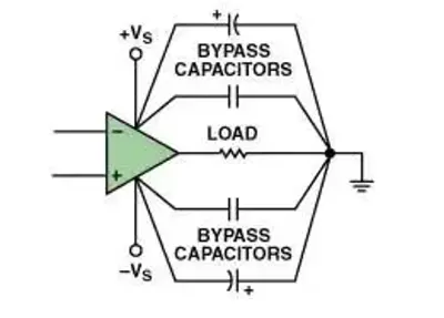
This method is the most effective in most cases and involves connecting the operational amplifier’s power supply pins directly to ground using multiple capacitors in parallel.
Generally, two capacitors in parallel are sufficient—though adding more parallel capacitors may offer benefits in certain circuits.
Parallel-connecting capacitors of different values helps ensure that the power supply pin experiences only very low AC impedance across a wide frequency range.
This is particularly important at the frequency where the operational amplifier’s power supply rejection ratio (PSR) begins to roll off.
These capacitors help compensate for the amplifier’s reduced PSR.
Maintaining a low-impedance ground path across many decades of frequency will help ensure that harmful noise cannot enter the operational amplifier.
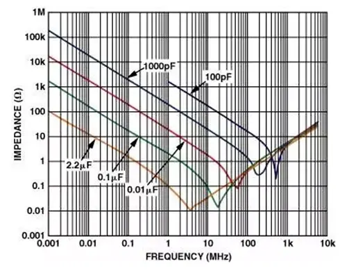
Figure 1 illustrates the advantages of using multiple capacitors in parallel.
At low frequencies, large capacitors provide a low-impedance ground path.
However, once the frequency reaches their own resonant frequency, the capacitance of the capacitors diminishes, and they gradually become inductive.
This is why using multiple capacitors is important.
When the frequency response of one capacitor begins to decline, the frequency response of another capacitor takes over.
This maintains very low AC impedance across many decades of frequency.
Practical PCB Placement Rules for Decoupling Capacitors
Start directly from the operational amplifier’s power supply pins;
Engineers should place the capacitor with the smallest capacitance and smallest physical dimensions on the same side of the PCB as the operational amplifier, and also position it as close to the amplifier as possible.
Engineers should connect the capacitor’s ground terminal directly to the ground plane using the shortest possible lead or trace.
This ground connection should be as close as possible to the amplifier’s load terminal to minimize interference between the power supply and ground terminals.
Figure 2 illustrates this connection method.
Repeat this process for capacitors with the next highest capacitance values.
It is best to start by placing a capacitor with a minimum capacitance of 0.01 µF.
We should also place a 2.2 µF (or slightly larger) low-ESR electrolytic capacitor nearby.
A 0.01 µF capacitor in a 0508 package offers very low series inductance and excellent high-frequency performance.
Power supply-to-power supply: Another configuration involves placing one or more bypass capacitors across the positive and negative power supply terminals of the operational amplifier.
This method is typically used when it is difficult to place four capacitors in the circuit.
The drawback is that the capacitor package size may increase, since the voltage across the capacitors is twice that of the single-supply bypass method.
The increased voltage requires a higher breakdown voltage rating for the components, which in turn necessitates a larger package size.
However, this method can improve PSR and distortion performance.
Because every circuit and layout is different, we must determine the capacitor configuration, quantity, and capacitance values based on the specific requirements of the circuit.
Parasitic Effects
Overview of Parasitic Effects in High-Speed PCB Design
Parasitic effects refer to those mysterious, headache-inducing glitches (in the literal sense) that sneak into your PCB and wreak havoc on the circuit.
They are hidden parasitic capacitance and parasitic inductance that infiltrate high-speed circuits.
These include parasitic inductance caused by excessively long package leads and printed traces.
They also include parasitic capacitance formed between pads and ground, pads and power planes, and pads and traces.
Mutual interference between through-holes is another factor.
There are many other possible parasitic effects as well.
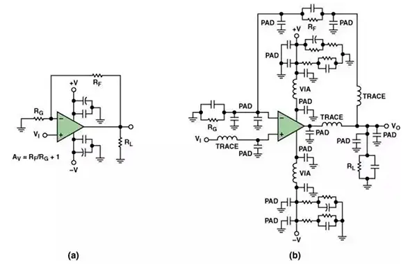
Figure 3(a) shows a typical in-phase operational amplifier schematic.
However, when parasitic effects are taken into account, the same circuit might look like Figure 3(b).
Impact of Small Parasitics on High-Frequency Stability
In high-speed circuits, even very small values can affect circuit performance.
Sometimes, a capacitance of just a few tens of picofarads (pF) is sufficient.
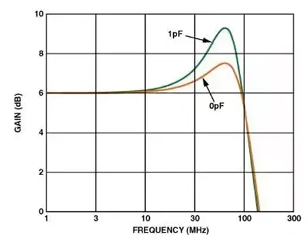
Related example: If there is only 1 pF of additional parasitic capacitance at the inverting input, it can cause a spike of nearly 2 dB in the frequency domain (see Figure 4).
If the parasitic capacitance is large enough, it can cause circuit instability and oscillation.
Modeling Parasitics: Capacitance, Trace Inductance, and Through-Holes
When searching for problematic sources of parasitic capacitance, you may find it useful to refer to a few basic formulas for calculating the values of the parasitic capacitances mentioned above.
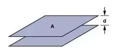
Equation (1) is the formula for calculating a parallel-plate capacitor (see Figure 5).
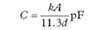
1) C represents the capacitance value, A represents the plate area in cm², k represents the relative permittivity of the PCB material, and d represents the distance between the plates in cm.
We must also consider strip inductance as a parasitic effect, which occurs when printed traces are excessively long or when a ground plane is absent.
Equation (2) shows the formula for calculating the inductance of a printed trace. See Figure 6.

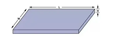
2) W represents the width of the printed line, L represents the length of the printed line, and H represents the thickness of the printed line.
All dimensions are in mm.
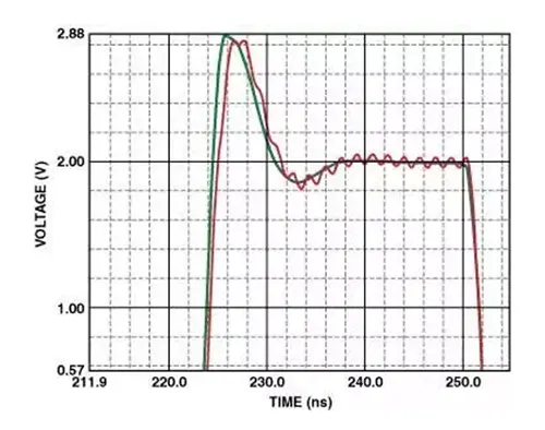
The oscillation shown in Figure 7 illustrates the effect of a 2.54 cm-long printed-circuit trace on the non-inverting input of a high-speed operational amplifier.
Its equivalent parasitic inductance is 29 nH (10⁻⁹ H), which is sufficient to cause sustained low-voltage oscillation that persists throughout the entire transient response cycle.
Figure 7 also shows how we can use a ground plane to reduce the effect of parasitic inductance.
Through-Hole Parasitics and Their Practical Design Implications
Through-holes are another source of parasitic effects; they can cause parasitic inductance and parasitic capacitance.
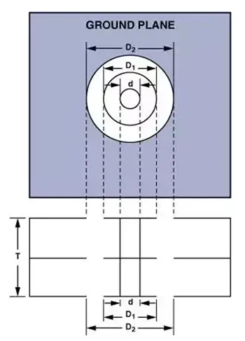
Equation (3) is the formula for calculating parasitic inductance (see Figure 8).
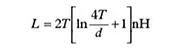
1) T represents the thickness of the PCB, and d represents the diameter of the through-hole in centimeters.
Equation (4) shows how to calculate the parasitic capacitance caused by through-holes (see Figure 8).
式4
2) εr represents the relative magnetic permeability of the PCB material.
T represents the thickness of the PCB. D1 represents the diameter of the pad surrounding the through-hole.
D2 represents the diameter of the isolation hole in the ground plane.
All dimensions are in cm. On a 0.157 cm-thick PCB, a single through-hole can introduce 1.2 nH of parasitic inductance and 0.5 pF of parasitic capacitance;
This is why it is essential to remain vigilant at all times when routing a PCB, in order to minimize the impact of parasitic effects.
Ground Plane
Role and Trade-Offs of Ground Planes in PCB Design
In reality, there is much more to discuss than what is covered in this article, but we will highlight some key characteristics and encourage readers to explore this topic further.
A ground plane serves as a common reference voltage, provides shielding, facilitates heat dissipation, and reduces parasitic inductance (though it also increases parasitic capacitance).
Although using a ground plane offers many benefits, care must be taken during implementation because it imposes certain limitations on what can and cannot be done.
Ideally, we should dedicate one layer of the PCB exclusively as a ground plane.
This ensures the best results as long as the entire plane remains intact.
Never repurpose areas of this dedicated ground plane layer to connect other signals.
Since a ground plane can eliminate the magnetic field between conductors and the ground plane, it can reduce the inductance of printed traces.
If we disrupt a section of the ground plane, it can introduce unexpected parasitic inductance into the printed traces above or below it.
Because ground planes typically have a large surface area and cross-sectional area, their resistance should be kept to a minimum.
At low frequencies, current follows the path of least resistance, but at high frequencies, it follows the path of least impedance.
Ground Plane Layout Strategy and Stability Considerations in High-Speed Circuits
However, there are exceptions; sometimes a smaller ground plane is preferable.
High-speed operational amplifiers perform better when the ground plane is moved away from the input or output pads.
This is because the parasitic capacitance introduced by the ground plane at the input increases the operational amplifier’s input capacitance, reducing phase margin and causing instability.
As discussed in the section on parasitic effects, even 1 pF of capacitance at the operational amplifier’s input can cause significant spike distortion.
Capacitive loads at the output—including parasitic capacitance—create poles in the feedback loop.
This reduces phase margin and causes the circuit to become unstable.
Whenever possible, we should separate analog and digital circuits, including their respective grounds and ground planes.
Fast rising edges can cause current spikes to flow into the ground plane.
The noise generated by these fast current spikes can degrade analog performance.
We should connect the analog ground and digital ground, as well as the power supplies, to a common ground point to reduce circulating digital and analog ground currents and noise.
High-Frequency Effects: Skin Effect and Conductive Losses
At high frequencies, a phenomenon known as the “skin effect” must be taken into account.
The skin effect causes current to flow toward the outer surface of a conductor—resulting in a narrowing of the conductor’s cross-sectional area and, consequently, an increase in DC resistance.
Although the skin effect is beyond the scope of this article, here is a good approximate formula for the skin depth in copper wire (in cm):
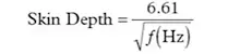
Electroplating with low-sensitivity metals helps reduce the skin effect.
Tracing and Shielding
Signal Integrity Challenges in Mixed-Signal PCB Design
PCBs carry a wide variety of analog and digital signals, ranging from high to low voltages or currents and from DC to GHz frequencies.
It is very difficult to ensure that these signals do not interfere with one another.
Recalling the recommendations from the previous section, “Trust No One,” the most critical step is to think ahead and develop a plan for how to handle signals on the PCB.
It is important to identify which signals are sensitive and determine what measures must be taken to ensure signal integrity.
We use a ground plane as a common reference point for electrical signals, and it can also provide shielding.
If we need signal isolation, we should first maintain physical distance between signal traces.
Layout Strategies for Reducing Coupling and Improving Isolation
Here are some best practices to follow:
Reducing the length of long parallel traces on the same PCB and minimizing the proximity between signal traces can reduce inductive coupling.
Reducing the length of long traces on adjacent layers can prevent capacitive coupling.
We should route high-isolation signal traces on different layers and, if complete isolation is not possible, we should route them orthogonally with a ground plane placed between them.
Orthogonal routing minimizes capacitive coupling, and the ground plane acts as an electrical shield.
We can use this method when we design controlled-impedance traces.
High-frequency (RF) signals typically travel on controlled-impedance traces.
That is, the trace maintains a characteristic impedance, such as 50 Ω (a typical value in RF applications).
The two most common types of controlled-impedance traces—microstrip 4 and stripline 5—can both achieve similar results, but through different methods.
We can place a microstrip controlled-impedance trace, as shown in Figure 9, on either side of the PCB.
It directly uses the ground plane beneath it as its reference plane.
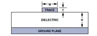
We can use Equation (6) to calculate the characteristic impedance of an FR4 board.
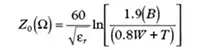
H represents the distance between the ground plane and the signal trace; W represents the trace width; and T represents the trace thickness.
All dimensions are expressed in mils (10⁻³ inches). εr represents the dielectric constant of the PCB material.
Controlled-Impedance Routing Structures and Design Trade-Offs
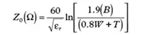
Strip-line controlled-impedance traces (see Figure 10) employ two ground planes with the signal trace sandwiched between them.
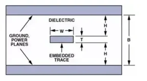
This method uses a larger number of traces, requires more PCB layers, is sensitive to variations in dielectric thickness, and is more expensive—so it is typically used only in applications with stringent requirements.
The formula for calculating the characteristic impedance of a stripline is shown in Equation (7).
Guard Rings and Local Shielding Techniques in Sensitive Circuits
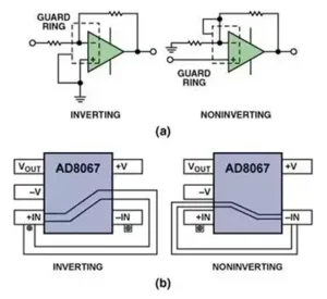
A guard ring, also known as an “isolation ring,” is another common shielding method used in operational amplifiers to prevent parasitic currents from entering sensitive nodes.
The basic principle is simple: a guard wire completely surrounds the sensitive node, and the wire maintains—or is forced to maintain—the same potential as the sensitive node (at low impedance), thereby diverting the absorbed parasitic current away from the sensitive node.
Figure 11(a) shows schematic diagrams of shield rings used in the inverting and non-inverting configurations of an operational amplifier.
Figure 11(b) illustrates typical routing methods for the two types of shield rings in an SOT-23-5 package.
Conclusion
PCB Layout Foundations for High-Speed Operational Amplifier Design
High-quality PCB routing is essential for successful operational amplifier circuit design, especially for high-speed circuits.
A well-designed schematic is the foundation of good routing; close collaboration between circuit design engineers and routing engineers is crucial, particularly regarding the placement of components and connections.
Factors to consider include power supply bypassing, minimizing parasitic effects, the use of ground planes, the impact of operational amplifier packages, and routing and shielding techniques.
Power Integrity and Bypass Capacitor Placement Strategy
1. We should place bypass capacitors at the chip power supply as close to the device as possible during PCB design; typically, we keep the distance under 3 mm.
2. Small ceramic bypass capacitors at the power supply pins of operational amplifier chips can provide energy for the amplifier’s high-frequency performance when the amplifier is processing high-frequency input signals.
We should select the capacitance value based on the input signal frequency and the amplifier’s speed.
For example, a 400 MHz amplifier might use a series connection of a 0.01 μF and a 1 nF capacitor.
3. When purchasing capacitors and other components, it is also important to consider their self-resonant frequency; capacitors operating near this frequency (400 MHz) offer no benefit.
Layout Rules for Parasitic Reduction and Signal Integrity
1. When designing a PCB, avoid routing other traces beneath the amplifier’s input and output pins or the feedback resistors.
This minimizes the mutual influence of parasitic capacitance between different traces, making the amplifier more stable.
2. Surface-mount components offer good high-frequency performance and are compact in size.
3. When routing traces on a circuit board, keep them as short as possible while also paying attention to their length and width to minimize parasitic effects.
Power Routing, Signal Sensitivity, and High-Speed Transmission Guidelines
1. When routing power lines, prioritize width as much as possible, since the worst parasitic characteristics of power lines are DC resistance and self-inductance.
2. The currents on amplifier input and output connection lines are very small, making them highly susceptible to interference; parasitic effects can be particularly harmful to them.
3. For signal paths longer than 1 cm, it is best to use controlled-impedance transmission lines terminated at both ends (with matching resistors).
Output Stability Techniques for Capacitive Loads
When an amplifier drives a capacitive-resistive load, a common technique to address stability issues is to introduce a resistor ROUT, preferably close to the op-amp, thereby using a series output resistor to isolate the capacitive load.