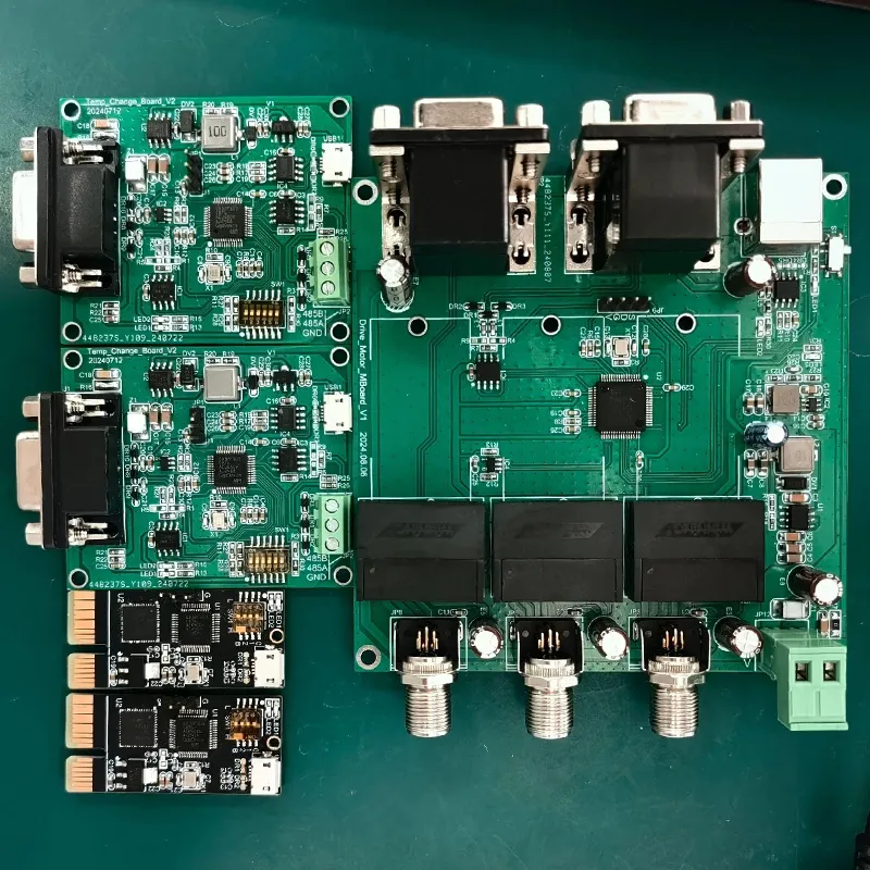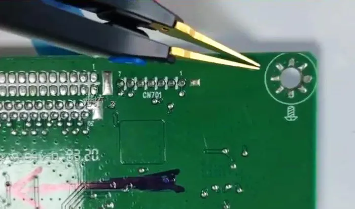
In actual production, PCBs are rarely 100% flat; they are almost always slightly warped to some degree. So, what is the standard for PCB warpage? Warpage is primarily assessed based on the “warpage degree.”
Causes of PCB warpage include: uneven stress, differences in thermal expansion, forces applied during the manufacturing process, and the materials themselves.
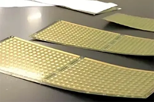
According to IPC standards, the warpage of a PCB intended for surface-mount assembly must be ≤ 0.75% to be considered acceptable.
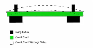
PCB Warpage: If the PCB warpage exceeds 0.75%, the board is deemed warped and fails inspection.
For PCBs that do not require surface-mount components (and contain only through-hole components), the flatness requirements are less stringent, and the warpage tolerance is relaxed to ≤1.5%.
However, in practice, to meet the demands of high-precision and high-speed placement, some manufacturers impose stricter requirements on PCB warpage, with some specifying a warpage of ≤0.5% and a few even requiring ≤0.3%.
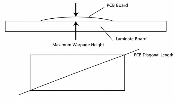
So how is PCB warpage calculated? Here is the formula.
Formula for Calculating PCB Warpage
The formula for calculating PCB warpage is as follows: Warpage = PCB Warpage Height / PCB Diagonal Length × 100%. For more details, see the figure below:
Areas for Improvement
Optimization of Base Materials and Auxiliary Materials
1. Board Material Selection
a. Prioritize core boards and prepregs with low CTE to match the expansion rate of copper foil and reduce thermal deformation.
b. For thick boards and high-layer-count boards, select high-rigidity FR-4 and high-TG materials to ensure high-temperature resistance and deformation resistance.
c. For boards with asymmetric structures, standardize the core board/PP type, thickness, and resin content.
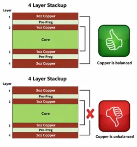
2. Balancing Copper Foil and Copper Thickness
a. Ensure the copper area on the top and bottom layers is as symmetrical as possible to avoid large areas of copper on a single side or localized thick copper.
b. Add grid copper or open-pattern copper in areas with thick copper to reduce concentrated stress in the copper layer.
3. Pre-preg (PP) Control
a. Use PP from the same batch and with the same resin content on the same board to minimize differences in curing shrinkage.
b. Use high-resin PP for boards requiring high flatness; use low-resin PP to reduce moisture-induced warpage.
PCB Layout Design Optimization
1. Interlayer Symmetry Design
a. Fully symmetrical stack-up structure: Core board thickness, number of PP layers, copper thickness, and trace distribution are mirror-image reflections of each other.
Large exposed areas on a single side and dense traces/pads on a single side are prohibited.
2. Copper Plating and Pattern Layout
a. Divide large, solid copper areas into a grid pattern, with the grid coverage ratio ≥30%, to relieve thermal stress.
b. Reserve stress relief slots and process openings along the board edges; prioritize adding slots along the long edges and on large boards.
c. Avoid large isolated copper patches around component areas and BGA regions.
3. Physical Dimensions and Panel Layout Design
a. For large and elongated boards, shorten the length of one side and divide the board and split units appropriately.
b. Use a combination of connecting strips and stamp holes in the panel layout to reduce deformation caused by pulling during board separation; avoid narrow, elongated contiguous sections.
When the board is relatively thin, increase the width of the process margin along the board edges to enhance overall rigidity.
4. Hole Design
a. Distribute flow-guiding holes and heat-dissipation holes evenly across large areas to ensure balanced heat distribution and exhaust.
Do not concentrate dense clusters of holes on a single side of the board.
Process Improvement
1. Process Improvement Areas in PCB Factories
Laminating process, front-end processes (material cutting, inner layers, etching), surface treatment processes, baking, etc.
2. Process Improvement Areas in SMT Operations
Optimization of oven temperature profiles, use of carriers/jigs, loading and handling processes, placement sequence and layout, press and bake processes, etc.
Conclusion
To sum up, PCB warpage directly affects assembly quality, especially SMT yield.
Following IPC standards, the acceptable warpage limit is 0.75% for SMT boards and 1.5% for through-hole boards, though high-speed placement applications demand stricter limits.
Warpage can be calculated by the ratio of warpage height to board diagonal length.
To control warpage, manufacturers should select low-CTE, high-TG core and prepreg materials.
They should also maintain symmetrical copper distribution and stack-up structures in the layout, optimize panel design and hole arrangement, and fine-tune lamination, baking, and SMT thermal profiles.
Combined material, design and process optimization can effectively balance internal stress and thermal deformation, reducing warpage to meet flatness requirements for different assembly applications.