The electronic information industry has evolved continuously for more than a century. Its underlying physical transmission mechanisms are now undergoing a historic paradigm shift.
Signal transmission is moving from traditional electrical conduction toward high-frequency electromagnetic field spatial coupling.
Large-scale artificial intelligence (AI) models, embodied intelligence, computing infrastructure, millimeter-wave radar, 5G/6G/terahertz communications, and quantum information are driving rapid technological advances.
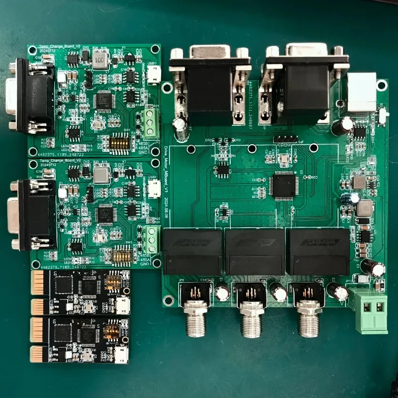
Printed circuit boards (PCBs) and semiconductor (integrated circuit, IC) packaging substrates have evolved beyond basic interconnection carriers.
They now serve as core strategic components that determine electronic systems’ performance, signal transmission quality, and long-term reliability.
Under low-frequency conditions, signals are transmitted via currents within conductors, and performance is determined by fundamental electrical parameters;
However, millimeter-wave and terahertz signals propagate through electromagnetic field coupling. System quality depends on the stability of the substrate’s dielectric constant and dielectric loss.
Conductor surface roughness and impedance matching also play critical roles. The system must also maintain precise control of the electromagnetic field across the entire structure.
This fundamental shift in physical mechanisms imposes revolutionary demands on the four major materials—conductors, dielectrics, reinforcements, and fillers—as well as on the entire manufacturing process.
This paper focuses on the transition from current-based transmission to electromagnetic field propagation.
It systematically analyzes industrial evolution, material upgrades, process innovations, and technological pathways.
It provides theoretical support and practical guidance for industry strategic planning, R&D strategies, and domestic substitution in China.
Stages of Development
Early Stage of Discrete Components
From the early 20th century through the 1950s was the era of discrete components. Vacuum tubes and transistors were gradually industrialized, and equipment was primarily used for low-frequency analog signal processing.
Signals relied entirely on the directional conduction of current within conductors, eliminating issues such as electromagnetic field losses and crosstalk. PCBs were primarily simple single-layer or double-layer structures;
The substrate material was phenolic resin, which served only the three basic functions of electrical insulation, structural support, and soldering fixation, with no high-frequency electrical requirements;
the manufacturing processes relied mainly on mechanical drilling and traditional wet etching.
Stages of Integrated Circuit Development
From 1960 to 2010, Moore’s Law dominated the semiconductor industry, and the integration density of integrated circuits continued to increase.
During this period, electrical signal transmission remained the primary method, but electromagnetic interference began to affect signal integrity.
PCBs evolved toward multilayer, high-density, and high-reliability designs, with FR-4 epoxy copper-clad laminate becoming the standard substrate.
The skin effect, signal crosstalk, and impedance discontinuities became more pronounced.
The industry adopted low-profile copper foil, high-temperature-resistant epoxy resin, polyimide (PI), and bismaleimide triazine resin (BT) for PCB manufacturing.
Processes have evolved to include laser precision drilling, fine-line routing, and high-density interconnect (HDI) layered manufacturing.
5G and Advanced Packaging
From 2010 to 2025, 5G base stations, AI computing servers, and in-vehicle millimeter-wave radars will see widespread adoption.
System operating frequencies will enter the 24, 28, 77, and 79 GHz millimeter-wave bands, leading to the large-scale deployment of millimeter-wave technology.
Electromagnetic field effects will become dominant, and signal transmission will shift entirely from conduction through wires to spatial propagation via electromagnetic waves.
High-frequency transmission losses are rising sharply. Heat flux density continues to increase.
High-density integration creates severe electromagnetic interference. Thermal expansion mismatches between heterogeneous materials can also cause delamination, warping, and reliability failures.
The materials system has undergone a comprehensive upgrade.
It now includes liquid crystal polymers (LCP), polytetrafluoroethylene (PTFE), low-loss hydrocarbon resins, low-dielectric-constant glass fiber, hyper-very-low-profile copper foil (HVLP), Ajinomoto build-up film (ABF), and nano-functional fillers.
Processing technologies are advancing toward ultra-fine circuits, ultra-thin substrates, ultra-flat conductors, direct copper-to-copper bonding, and precision TSV filling;
System performance is directly determined by electromagnetic field propagation characteristics, dielectric constant (Dk), and dielectric loss (Df) metrics, as well as the surface condition of the conductors.
6G and Terahertz Era
Starting in 2025, 6G, terahertz communications, quantum information, and embodied intelligence will advance into pre-industrial research and early commercial deployment, while communication systems will increasingly operate in the sub-terahertz and terahertz frequency bands.
Electronic circuit substrates will evolve into composite microsystems that integrate electromagnetic control, efficient thermal management, structural support, shielding and protection, and heterogeneous interfacing.
Signals will exhibit characteristics of multi-physics coupling involving photonic, electronic, and electromagnetic fields, with transmission loss, dispersion, latency, heat dissipation, and reliability simultaneously approaching physical limits.
The core of industry development will hinge on achieving synergistic matching of multi-field properties—including electrical, magnetic, thermal, mechanical, and optical—at the atomic scale through advanced materials.
Upgrade Requirements
Conductor Copper Foil Materials
The skin effect is significantly exacerbated under high-frequency and terahertz conditions; the skin depth of a copper conductor at 100 GHz is only 0.1–0.2 μm;
Traditional roughened copper foil has a surface roughness of 1.0–3.0 μm, which causes a sharp increase in high-frequency losses.
The industry needs to adopt HVLP (Ultra-Low Profile) copper foil with a surface roughness of Ra ≤ 0.1 μm, which can limit conductor losses at 100 GHz to within 0.3 dB/cm.
Ultra-low-profile copper foil with a roughness of Ra = 0.08 μm can reduce high-frequency losses by more than 70% compared to conventional copper foil with a roughness of Ra = 1 μm.
AI chips and flip-chip ball grid array (FC-BGA) packages demand higher current density, stronger electromigration resistance, and greater high-temperature reliability from conductors.
These requirements are driving research into graphene-composite copper, nanotwin copper, and low-temperature copper-copper bonding technologies.
Terahertz and quantum computing applications are driving interest in superconducting interconnect materials, low-dimensional conductive electrodes, and ultra-high-purity non-magnetic conductors.
These materials require extremely low interface defect densities and minimal electromagnetic noise to support reliable performance.
Insulating Dielectric Materials
6G millimeter-wave applications require a dielectric with Dk = 2.5–3.2 and Df ≤ 0.0010 (10–100 GHz); terahertz applications require Df ≤ 0.0008 (300 GHz).
Conventional FR-4 has relatively high dielectric loss and cannot meet the requirements of next-generation high-frequency systems.
As high-end AI chips generate heat flux densities above 1,000 W/cm², dielectric materials must provide both high thermal conductivity and a low coefficient of thermal expansion.
A thermal conductivity of 1.5–5.0 W/(m·K) and thermal expansion compatible with silicon and copper can help suppress warping, delamination, and material failure.
Package dielectric thickness has been reduced to 5–20 μm, requiring high strength, low stress, low water absorption, and excellent laser micro-drilling performance.
Mainstream materials include LCP, modified PTFE, hydrocarbon resins, ABF, and low-dielectric resins such as polyphenylene ether (PPE) and polyphenylene oxide (PPO).
Structure-Reinforced Substrates
Traditional E-glass fibers have a relatively high dielectric constant and are not suitable for high-frequency, high-speed applications.
The new generation of reinforcing materials includes NE low-dielectric glass fibers, S-glass fibers, quartz fibers, aramid fibers, and hollow porous glass fibers.
These materials must achieve Dk ≤ 4.5, Df ≤ 0.001, and a CTE of 3–5 × 10⁻⁶/°C.
They also need to support ultra-thin, lightweight designs while maintaining low moisture absorption and high dimensional stability.
NE low-dielectric glass fiber has a Dk of 4.2, a Df of 0.0009, and a CTE of approximately 4 × 10^(−6)/°C, enabling long-term stable operation of 6G and terahertz substrates.
Functional Filler Materials
Nanofillers have evolved from cost-saving agents to core functional materials that regulate dielectric properties, thermal conductivity, thermal expansion, mechanical strength, and flame retardancy.
Mainstream fillers include nano-silica, boron nitride, aluminum oxide, diamond micropowder, and graphene thermal conductive fillers.
These materials must exhibit uniform nanoscale dispersion, low polarity, low moisture absorption, excellent interfacial compatibility, and no increase in dielectric loss.
Adding 15% nano-boron nitride can increase the substrate’s thermal conductivity to 4.8 W/(m·K) while maintaining a low loss level of Df ≤ 0.001.
Era of Electromagnetic Fields: A Disruptive Upgrade in Electronic Circuit Manufacturing Processes
Ultra-Fine Precision Circuits and Ultra-Flat Conductor Processes
High-frequency PCBs with line widths and spacings of ≤5 μm require advanced manufacturing techniques.
Terahertz applications require even finer dimensions of ≤2 μm.
Manufacturers use laser direct imaging (LDI), digital printing, precision electroplating, precise micro-etching control, and ultra-smooth conductor finishing to minimize line side etching and control surface roughness.
Atomic-Level Thin Film Deposition and Precise Control of Heterogeneous Interfaces
Using atomic layer deposition (ALD), atomic layer etching (ALE), and molecular beam epitaxy (MBE) to achieve single-atom-layer thin film fabrication.
These techniques create metal barrier layers, conductive seed layers, and surface passivation layers.
These layers help prevent interface defects, metal diffusion, oxidation-induced degradation, and impedance drift at their source.
High-Precision Laminating and Dynamic Warpage Control Process for Substrates
Ultra-thin substrates with a thickness of ≤50 μm and high-layer-count substrates with 20 to 40 layers.
A low-temperature, low-pressure precision lamination process is employed to strictly control the Z-axis expansion rate and overall warpage, thereby ensuring packaging and assembly accuracy as well as long-term reliability.
Precision Laser Micro-Blind Hole Machining and High Aspect Ratio Hole-Filling Process
Microholes have diameters ranging from 20 to 50 μm, with a machining accuracy of ±5 μm.
The high aspect ratio hole-filling process produces holes free of voids and gaps, meeting the high-density interconnect requirements of high-end HDI and IC packaging.
·Integrated Electromagnetic Shielding and Integrated Thermal Management Synergistic Process
The integrated manufacturing process combines embedded shielding, nano-conductive shielding coatings, highly thermally conductive through-holes, and graphene-composite heat dissipation layers.
Together, these technologies improve electromagnetic compatibility and heat dissipation under high heat flux densities.
Green, Low-Carbon, and High-Reliability Manufacturing Processes
The industry is adopting lead-free, halogen-free, and low-VOC green manufacturing processes.
These processes improve the substrate’s resistance to conductive anodic filaments (CAF) and high- and low-temperature cycling while extending its service life.
As a result, manufacturers can meet the high-reliability requirements of telecommunications, automotive, and computing equipment.
Industry Development Trends and Strategies for Collaborative Responses Across the Entire Supply Chain
·Shifting from the Optimization of Single Materials to Collaborative, System-Wide Design Across All Materials
Future competition will depend less on improving individual material performance and more on achieving comprehensive and compatible system-level design.
Engineers must coordinate electrical properties, thermal expansion, electromagnetic fields, and processing techniques across conductors, dielectrics, reinforcements, fillers, and interfaces.
This collaborative approach will enable better overall material-system performance.
Shifting from Trial-and-Error R&D to Precise Reverse Design via AI-Driven Materials Genomics
Machine learning, molecular dynamics simulations, and high-throughput materials screening can enable reverse engineering of material formulations.
Engineers can tailor these formulations to target Dk/Df, heat resistance, thermal conductivity, thermal expansion, and mechanical properties.
This approach can significantly shorten R&D cycles and reduce trial-and-error costs.
Shifting from Independent PCB Manufacturing to a Chip-Package-Substrate Co-Design Model
The industry should adopt system-technology co-optimization (STCO), system-process co-optimization, design-technology co-optimization (DTCO), and design-process co-optimization.
It should also integrate material parameters into the early design of chiplets, 3D stacks, and co-packaged optics (CPO) architectures to optimize overall system performance.
Accelerate the Domestic Production of Core Materials and Build an Independent and Controllable Supply Chain
The industry should prioritize key technological breakthroughs to achieve domestic production of ultra-low-profile copper foil, high-frequency low-loss resins, low-dielectric-constant glass fiber, nano-functional fillers, ABF packaging dielectrics, and high-end ultra-thin copper foil.
These advances will strengthen the independence and controllability of the domestic supply chain.
Phased Development of Specialized Materials for 6G, Terahertz, and Quantum Technologies
Short Term (2026–2030): Achieve breakthroughs in the domestic production of low-loss substrates, HVLP copper foil, nanofillers, and ABF materials;
Medium Term (2030–2035): Develop specialized substrates for terahertz applications, flexible and stretchable substrates, and integrated high-thermal-conductivity composite substrates;
Long Term (2035 and beyond): Develop smart tunable dielectric materials, self-healing materials, superconducting interconnect materials, and quantum-level ultra-low-noise substrate systems.
Conclusion
The electronic information industry has fully entered a new era dominated by electromagnetic fields across the board, with PCBs and packaging substrates becoming the core strategic drivers that determine the upper limits of system performance.
The industry’s core bottlenecks have shifted from chip manufacturing processes to material systems and precision manufacturing capabilities.
The four major material systems—conductive copper foil, insulating media, structural reinforcements, and functional fillers—provide the physical foundation for electromagnetic field propagation.
Together, these materials directly influence system transmission loss, signal delay, bandwidth capacity, thermal power consumption, and long-term reliability.
In the future, competition in the global electronics and information technology industry will fundamentally revolve around comprehensive, systematic competition in material systems, heterogeneous interfaces, atomic-level manufacturing, and multi-physics field coordination.
We must adhere to full-chain collaborative innovation and implement the overarching principle that “materials define performance, processes support limits, design aligns with application scenarios, and applications drive iteration.”
Overcoming the four major bottlenecks—the frequency barrier, the loss barrier, the power consumption barrier, and the integration barrier—will help the electronic circuit industry build an autonomous, controllable, and globally leading ecosystem.
This progress will also establish a solid physical foundation for artificial intelligence, 6G terahertz communications, quantum information, embodied intelligence, and integrated air-space-ground information networks.