Six Things to Consider When Transferring a PCB Schematic to Layout Design. All the examples mentioned were developed using the Multisim design environment, but the same concepts apply when using different EDA tools!
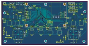
When a schematic is transferred to the layout environment via a netlist file, component information, the netlist, layout information, and the initial trace width settings are also transferred.
Recommended Steps for the Layout Design Phase
1. Set the grid and unit values appropriately. To achieve more precise layout control over components and traces, set the component grid, copper fill grid, via grid, and SMD grid to 1 mil.
2. Set the PCB outer margin and via dimensions to the required values. PCB manufacturers may have specific minimum values or recommended nominal values for blind and buried vias.
3. Set the appropriate pad/via parameters based on the PCB manufacturer’s capabilities. Most PCB manufacturers support small vias with a drill diameter of 10 mil and a pad diameter of 20 mil.
4. Set design rules as required.
5. Set custom shortcut keys for frequently used layers so you can quickly switch layers (and create vias) during routing.
Handling Errors During Schematic Transfer
A common error during schematic transfer is the absence of or incorrect package assignments.
Please note:
If a component in the schematic lacks a package, an alert message will pop up indicating that the virtual component cannot be exported.
In this case, since no default package information is transferred to the layout, the component will simply be removed from the layout.
If a package is transferred but cannot be correctly matched to a valid package shape, an alert message indicating a mismatch will also be generated during the transfer process.
Correct the package assignments in the schematic, or create a valid package for any components.
After making the corrections, perform the forward annotation step to update and synchronize the design information.
Updating the Design Through Annotation
Annotation is the process of transferring design changes from the schematic to the layout, or from the layout to the schematic.
Backward annotation (layout to schematic) and forward annotation (schematic to layout) are key to maintaining design accuracy.
To protect your work, back up and archive the current versions of the schematic and layout files before performing any significant forward or backward annotation steps.
Do not attempt to make changes to both the schematic and layout simultaneously.
Make changes to only one part of the design (either the schematic or the layout), and then perform the appropriate annotation steps to synchronize the design data.
Component Renumbering
Component renumbering is a feature that renumbers the components on a PCB in a specific order. Reference designations should be arranged in a top-to-bottom, left-to-right order on the PCB.
This makes it easier to locate components on the board during assembly, testing, and troubleshooting.
Handling Last-Minute Component or Netlist Changes
Last-minute changes to PCB components or netlists are not recommended, but sometimes they are unavoidable due to component availability issues or the detection of last-minute design errors.
If the change involves a component or the netlist, it should be made in the schematic and then forward-referenced into the layout tool.
Here are some tips:
1. If you add a new component after layout has begun (such as a pull-up resistor on an open-drain output), add the resistor and its network to the design in the schematic.
After forward annotation, the resistor will appear as an unplaced component outside the PCB boundary, with a flyline indicating the network connection.
Next, move the component inside the PCB boundary and route it as usual.
2. Backward annotation works well in conjunction with reference number changes, such as renumbering during post-layout.
Locating Components Using Highlight Selection
During the PCB layout process, one way to locate specific components or traces in the schematic is to use the “Highlight Selection” feature.
This feature allows you to select a component or a trace (or multiple objects) and then view their locations in the schematic.
This feature is particularly useful for matching bypass capacitors to their corresponding IC connections.
Conversely, it can also be used to locate specific components or traces on the layout while viewing the schematic.
Conclusion
To sum up, successful schematic-to-layout PCB conversion relies on standardized pre-setup, disciplined data synchronization, and proper handling of unexpected design adjustments.
Engineers need to configure grids, board outlines, via/pad specifications, and design rules in advance according to PCB manufacturing capabilities.
When encountering transfer failures caused by missing or mismatched footprints, corrections should be completed in the schematic before executing forward annotation.
Bidirectional annotation serves as the foundation for keeping schematic and layout data synchronized; designers must avoid parallel edits on both documents and complete file backups before major updates.
Rational component renumbering improves manufacturability and debug efficiency, while all last-minute netlist or component revisions should originate from the schematic and be synchronized into layout.
Functions such as highlight selection further streamline cross-referencing between schematic and layout.
Following these practices effectively reduces data discrepancies, improves layout efficiency, and supports reliable, manufacturable PCB development regardless of the EDA tool in use.