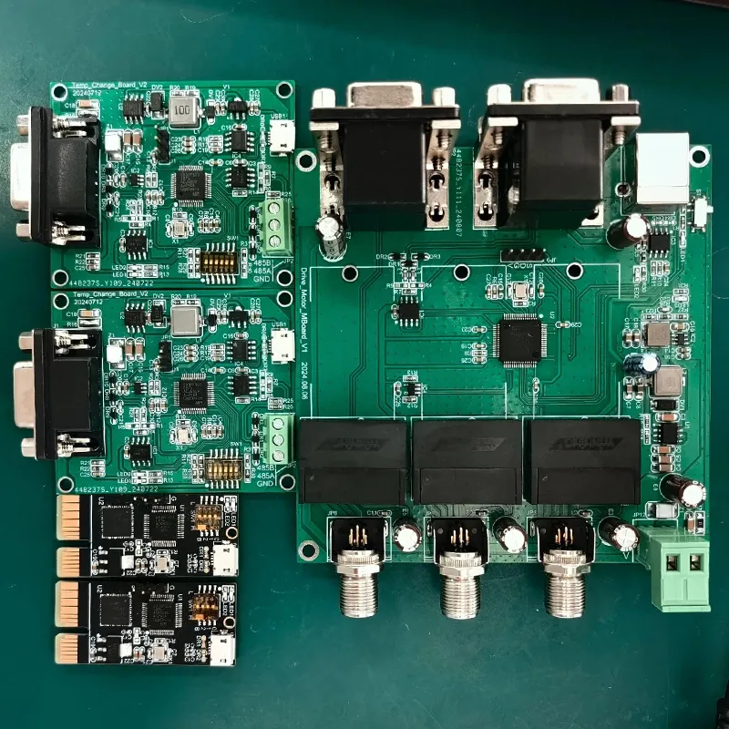
When printed circuit boards first appeared on the market, they were almost exclusively designed using traditional through-hole technology.
At that time, all boards had to undergo wave soldering, and they were single-sided.
Later, after the invention of SMD component technology, a hybrid approach combining SMT and wave soldering began to emerge.
However, a significant portion of the components at that time could not be converted to the SMD process.
This meant a hybrid approach was necessary, combining traditional through-hole and SMD components.
After the SMT process was completed, the board underwent a manual through-hole insertion step, followed by wave soldering.
Due to these process requirements, the board design had to place all through-hole components on one side, while the other side was reserved for wave soldering.
The SMD components on the side undergoing wave soldering had to be secured with red adhesive to prevent them from falling off during the wave soldering process.
Precautions for the Wave Soldering Process
1. For areas to be wave soldered, it is best to fill the through-holes (vias) to prevent solder from overflowing onto the component surfaces as they pass through the wave soldering bath, which could cause unpredictable short circuits.
2. For components with pin arrays, the pins should be aligned parallel to the direction of the wave soldering process.
This prevents short circuits between pins and ensures better solder coverage.
3. If small SMT components such as resistors, capacitors, or inductors need to undergo wave soldering, they should be oriented perpendicular to the direction of the wave soldering process.
4. For SOICs (ICs with leads on both sides of the package), the entire row of leads should be parallel to the direction of the wave soldering process.
5. Please note that only single-row or dual-row lead components are suitable for wave soldering;
Components with leads on all four sides are not suitable for this process.
6. To avoid shadowing effects, taller and larger components should be positioned toward the rear in the direction of the wave soldering process.
Recommendations for Hand Placement During Wave Soldering
1. Insert tight-fitting components first, such as connectors with bent pins that connect to the outside world.
This prevents other components that have already been inserted from falling out due to vibration when inserting the tight-fitting ones.
2. When inserting components, arrange the right-hand insertion positions from top-left to bottom-right, and the left-hand insertion positions from top-right to bottom-left, to prevent components from obstructing hand movements.
3. Insert components in order from the lowest to the highest to prevent taller components from obstructing hand movements. (For example, a resistor between two connectors.)
4. It is best to insert identical components at the same station. (This reduces the chance of misplacement or using the wrong component.)
5. Components inserted by the same operator should ideally be concentrated in one corner, allowing the operator to focus their eyes on a single area and thereby minimize errors.
6. Components that look identical but have different part numbers should be avoided at the same workstation as much as possible to prevent confusion.
7. Polarized components should be avoided at the same workstation whenever possible.
Otherwise, the workload at that station will become too heavy.
8. Efforts should be made to ensure that each workstation has the same processing time.
Conclusion
The wave soldering process has played an important role in PCB assembly, especially during the transition period from traditional through-hole technology to modern SMT manufacturing.
Although many components have now shifted to surface mount technology, wave soldering remains widely used for specific through-hole components and mixed-technology PCB assemblies.
To achieve reliable soldering quality, PCB designers and manufacturers must carefully consider component layout, soldering direction, component height, and placement sequence.
Proper design practices, combined with optimized hand insertion procedures, can help prevent solder defects such as bridging, insufficient solder coverage, and component misplacement.
By following appropriate wave soldering process guidelines and assembly recommendations, manufacturers can improve production efficiency, reduce manufacturing risks, and ensure higher-quality PCB products for various electronic applications.