PCB stackup refers to the structured arrangement of copper and insulating layers in a printed circuit board, and it plays a critical role in determining the performance of modern electronic systems.
With the increasing demand for smaller, faster, and more reliable devices, multilayer PCB designs have become essential.
A well-planned stackup helps reduce electromagnetic interference (EMI), improve signal integrity, and control impedance and crosstalk, making it a key foundation in high-speed and high-density PCB design.
What is a PCB Stackup?
A PCB stackup refers to the arrangement of copper layers and insulating layers that make up a PCB prior to the layout design.
A PCB stackup helps minimize the circuit’s susceptibility to external noise, as well as minimize signal amplitude and reduce impedance and crosstalk issues in high-speed PCB layouts.
For the design of compact electronic products, engineers generally recommend using PCBs with multi-layer and 3D designs. The figure below shows an example of an 8-layer PCB stackup:

For multilayer PCBs, three main types of layers are used: signal layers, ground planes, and mixed layers. Signal layers consist of various types of signals. Here is a brief introduction to each of these three layers.
Signal Layer
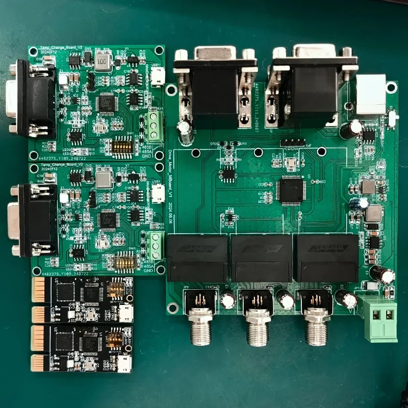
The image below shows a well-designed signal layer PCB that accommodates various types of signals without relying on any specific standard.
It primarily handles low-voltage, low-current signals used for transmitting medium- to high-speed data.
This type of layer does not include ground or power planes formed by polygon fills.
This is because, in very high-speed signals, the presence of ground or power planes can cause impedance variations due to the accumulation of stray capacitance and stray inductance.
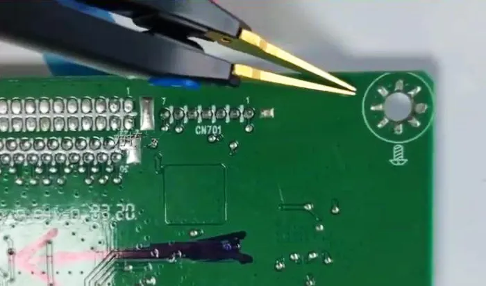
The figure below shows a signal layer with multiple signals routed and components placed.

Ground Plane
A ground plane is different in that it does not carry any signals other than ground or power.
It serves several purposes, primarily to ensure good ground and power paths throughout the circuit. Solid copper is placed across the entire board;
By simply cutting through the copper plane, separate sections can be created to provide different ground signals.
Below is a good example showing a ground plane.

Mixed Layer
The next type of layer is the mixed layer, which uses signal traces and copper fill as its plane.
This is the most common layer type in two-layer and six-layer boards, and it is sometimes used in four-layer boards as well.
Mixed layers are found on standard PCBs that do not have any obvious high-speed traces.
The image below shows an example of a mixed layer.

Why is PCB Layering Necessary?
Evolving Demands
As technology continues to advance, the demands placed on electronic products are becoming increasingly stringent.
There is a growing need for PCBs that are small and lightweight, yet offer superior functionality, reliability, and longevity.
This has led to the development of multilayer PCBs.
A multilayer PCB is created by stacking two or more single-sided and/or double-sided PCBs together, with reliable, predefined interconnections between them.
A multilayer PCB consists of three or more conductive layers, with two outer layers and an insulating layer in between.
As PCB complexity and density increase, issues such as noise, stray capacitance, and crosstalk may arise when the layer stacking design is inefficient.
PCB Stack-Up Determines EMC Performance
PCB stackup is one of the most critical factors in determining a product’s electromagnetic compatibility (EMC) performance.
A well-designed stackup can minimize radiation and protect circuits from interference caused by external noise sources.
It can also reduce issues such as signal crosstalk and impedance mismatch.
However, a poorly designed stackup can lead to increased EMI (electromagnetic interference) radiation, as impedance mismatch causes reflections and ringing within the system, which can significantly degrade product performance and reliability.
PCB Stackups can Maintain Signal Integrity
PCB stackups can be designed to include features that help maintain signal integrity.
Maximum capacitive decoupling in power distribution networks is achieved by placing the power plane directly adjacent to the ground plane within the stackup. Signal layers or PCB layers should always have an adjacent ground plane within the PCB stackup.
Including a ground plane next to each signal layer enhances magnetic flux cancellation and eliminates noise.
Minimizing the spacing between conductive PCB layers increases flux cancellation.
High-speed traces are best routed in ribbon traces to maximize the shielding and flux cancellation provided by adjacent ground planes.
Less sensitive traces with a lower risk of air coupling are best routed on the outer layers of the printed circuit board.
Further routing techniques combine the aspect ratio of the chassis connections with the ground pins between each layer.
Ground fills between outer-layer traces with a large number of ground pins provide return paths and mitigate the generation of loop currents.

PCB Layers to Avoid Discontinuities and Loops
Use a layout that minimizes RF energy by avoiding unnecessary impedance and unnecessary materials, such as excessively thick copper.
Design the PCB stackup to eliminate impedance buildup and divert RF energy to the chassis.
Route signals to ensure that return paths are located directly beneath the signal traces. Avoid impedance loops on the PCB when fast-switching signals are present.
Evaluate PCB layers when placing buried vias to ensure there are no discontinuities.
Discontinuities create gaps in the layer plane and may force return paths into noise-generating loops.
Place decoupling capacitors on the power rails of each component to shunt switching signals to ground, and place bypass capacitors on switching signals at connectors entering and exiting the design.
PCB Stack-Up for Capacitive Decoupling and Magnetic Flux Cancellation
Arrange the power and ground planes adjacent to each other to ensure clean power distribution across the entire PCB layer.
When the power and ground planes are adjacent in the stackup, low-impedance capacitive decoupling results in clean power distribution.
Continue to ensure the integrity of the power distribution network across the entire layer by adding decoupling capacitors at the power leads of each component connected to the PCB layer.
Designing decoupling capacitors around each component’s power leads provides power to large digital networks that switch simultaneously.
Adding decoupling capacitors at signal pins that undergo transitions during clock cycles ensures power distribution integrity across the entire layer.
Decoupling and bypass capacitors provide sufficient power to maintain expected signals during operation, preventing ground bounce and the unintended injection of RF energy into the PCB layer.

PCB Stack-Up: Avoiding Unwanted Impedance and Loops
Layer signal planes adjacent to ground planes to prevent the formation of loops that generate RF energy.
When the return plane is directly adjacent to the signal plane, no loop is formed.
Via placement is critical for avoiding slots in the layer stack, where signals may need to propagate around the slot, thereby creating loops.
Additionally, high-speed signals generate flux in both the signal network and the return network.
This flux is equal and opposite in the signal and return paths.
Maximum cancellation occurs when high-speed signals and the return path are placed directly adjacent to each other.
The magnetic flux generated by high-speed signals must be eliminated to maintain electromagnetic compatibility (EMC).
Design the PCB stackup to ensure that the return plane is adjacent to each signal layer, thereby achieving electromagnetic compatibility (EMC).
EMC indicates that the stackup is designed to properly minimize the generation of magnetic flux.
Differences Between Standard Laminates and HDI Laminates
There are fundamental differences between standard laminates and HDI laminates.
For standard laminates, factors to consider include: the number of layers, circuit frequency, and emission requirements.
Other parameters related to standard laminates include: the spacing between layers and shielded or unshielded areas.
Design rules are crucial for standard laminates. These rules include maintaining spacing between signal layers and using large core areas to mitigate EMC issues.
Another point worth noting is the benefit of standard laminates: using ground planes on the outer layers to protect the inner layers.
A drawback is that ground planes become smaller due to the presence of component mounting pads, particularly on high-density PCBs.
HDI stacking technology is transforming the manufacturing and design of multilayer PCBs.
Unlike standard stacking, HDI stacking offers more design options.
Furthermore, if you wish to simplify the design of complex boards, HDI stacking is the right choice.
Factors determining the stackup include: the number of signal layers, as well as the number of ground and power layers.
An important point to note is that these layers should be arranged symmetrically.
The fact that HDI does not require a complex architecture is a major advantage for designers.
PCB Layering Methods
Each layer of a PCB can only accommodate a limited number of traces, so the more networks in a design, the more layers are required for routing.
However, before you start adding layers to your design, it’s important to take a step back and look at the bigger picture.
The first detail you should consider is the manufacturing of the PCB itself.
The number of layers in a PCB is influenced by—and will influence—factors such as materials, manufacturability, and construction costs.
Materials
The number of standard digital and analog PCBs manufactured using FR-4 is well-known, but if your PCB uses more specialized high-speed materials, changing the number of layers becomes more challenging.
While these materials offer superior performance in terms of controlled impedance, signal integrity, dimensional stability, and thermal management, they can be difficult to work with and result in higher PCB manufacturing costs.
Before adding additional layer pairs.

Manufacturability
The higher the number of layers in a circuit board, the more complex the manufacturing process becomes.
This not only affects the time and cost required to manufacture the original circuit board but may also impact the production volume promised by the manufacturer.
Cost
Every layer added to a circuit board increases its cost. Generally speaking, manufacturing costs can rise by up to 40% when moving from two layers to four, or from four to six.
After that, the increase drops slightly to 35% or 30%, but it will still impact your bottom line.
While this may not seem like much during the prototyping phase, keep in mind that this cost will carry over into the production phase.
On the other hand, in some cases, adding layers can actually save you money.
Depending on the complexity of the routing in your design, adding extra layers may ultimately save you money and reduce development time.
Additional layers also allow you to adjust the number and size of vias, trace widths and spacing, as well as the board size and thickness—all of which can save on manufacturing time and costs.
Using additional layers may also end up being the only way to incorporate more components into your design.

Signal Routing
For designs with extensive networks, multi-layer printed circuit boards are often the only viable option for routing traces.
Additionally, extra layers can help with the following:
Crosstalk: When all traces are crowded onto a single layer, they may couple with one another and generate noise.
Adding layers to the board allows these sensitive networks to be spaced apart and routed vertically on adjacent layers.
EMI: Additional layers allow designers to separate the signal layers from the ground planes, thereby reducing EMI susceptibility and radiation.
High-Speed: Transmission line routing can also benefit from additional layers if they are used as reference planes to ensure a clean signal return path.
Power Planes and Ground Planes
Many components on a printed circuit board (PCB) require multiple voltage levels to meet their power requirements.
Maintaining good power integrity on a two-layer PCB can be challenging, as all these power sources must be routed through separate traces.
Utilizing additional layers on the PCB for extra power planes helps address this issue.
Even when there are multiple voltage levels on the board, power planes can be divided to manage the varying power requirements of the components.
One of the primary benefits of adding extra layers to a PCB is the ability to configure multiple ground planes.
In addition to helping improve the board’s power distribution network, ground planes serve as reference planes for signal return paths.
In two-layer designs, these return paths are typically limited to ground traces, which can lead to numerous signal integrity issues on the board.
However, with dedicated reference planes in multilayer boards, high-speed traces can be routed on layers directly adjacent to their reference planes to ensure clean signal returns.
Signal Integrity
High-speed designs typically require microstrip or stripline layer configurations to route sensitive transmission lines.
While microstrip configurations are routed on outer layers, stripline configurations require internal routing layers and ground planes, which can only be achieved through multilayer designs.
You can see some examples of these PCB layer configurations in the figure below.
Once upon a time, increasing the number of layers in a multilayer PCB was simply a matter of creating space for routing additional networks.
However, today it is essential to design a well-structured multilayer stackup to protect the PCB from external noise sources and prevent the PCB from propagating them.
Next, we will explore some PCB stackup techniques available for multilayer designs.

Case Study: PCB Stack-up (4-Layer)
For 4-layer boards, there are essentially two methods for creating the stack-up.
1. You can use two cores, drill and plate them separately, bond them together with prepreg, and then perform the final drilling and through-hole plating.

Most PCB design software, including the Proteus Design Suite, refers to this type of stackup as an “outer-layer pair” because the core is built from the outside in.
2. A drilled and plated core can be used. Then, a layer of prepreg/foil is placed on either side of the board, followed by curing, etching, drilling, and plating.

As expected, this is commonly referred to as an “internal layer pair,” since the core is built from the inside out.
When building a multilayer PCB, each drill span must pass through a separate CNC drill.
This means that once the layer stackup is defined, there is a set of known, valid drill spans that are possible.
For example, in the 4-layer board discussed earlier, if you use two cores (outer layer pairs), you might have three drilling spans, or if you use one core (inner layer pair), you might have two drilling spans.
Steps for PCB Layer Stackup Design
How Many Layers Are Needed?
Before deciding on the layer stackup, the first question is how many layers the design requires.
A standard rule of thumb is to use the number of pins per unit area on the PCB.
You need to consider the following:
Power (for high-power boards or when your circuit includes power supplies)
Ground planes/layers
Signals (low-speed or high-speed)
Ideally, the best design should not mix signal types within the core layers.
To determine the optimal number of layers, you can first calculate the pin density using the following formula:
Pin density = Board area / (Total number of pins / 14)
Once you have the pin density, use this lookup table to determine the number of signal layers.
| Pitch (mm) | Number of Signal Layers | Number of Board Layers |
|---|---|---|
| > 1.0 | 2 | 2 |
| 0.6 – 1.0 | 2 | 4 |
| 0.4 – 0.6 | 4 | 6 |
| 0.3 – 0.4 | 6 | 8 |
| 0.2 – 0.3 | 8 | 12 |
| < 0.2 | 10 | 14 |
PCB density depends on factors such as component placement and signal integrity.
Now that you’ve determined how many layers are needed, it’s time to decide which layers will carry which types of signals.
Before making these decisions, there are a few things to consider.
It’s important to route high-current signals on the top and bottom layers, as inner layers cannot dissipate heat through the air.
Therefore, using inner layers for high-current operations can cause the PCB temperature to rise.
High-frequency signals generate high levels of EMI, so stacking ground planes on the top and bottom layers of the PCB helps reduce radiated EMI.
Determining Layer Arrangement
Next, determine the number of layers and their arrangement. Follow these rules:
Avoid placing two signal layers side by side
Keep the stackup symmetrical from the top and bottom layers inward
Route high-speed signals on microstrips with the minimum thickness
Maintain the minimum spacing between power and ground layers
Keep internal power layers adjacent to signal layers to achieve tight coupling
Determining Layer Material Types
Next, determine the thickness of each signal layer, including the core and prepreg.
Although there are standard thicknesses for PCB materials, you should consider the thermal, electrical, and mechanical properties of each material.
Determining Routing and Via Placement
Finally, determine the routing paths by making the following decisions:
- Copper weighting
- Where to place vias
- Via type

Dielectric and Copper Density and Layer Management
Before proceeding with PCB design, dielectric and copper density are other important criteria to consider when making design decisions.
This is because changing the copper density and dielectric material alters the board dimensions and may affect the impedance parameters of the entire board.
Copper density and PCB dimensions also influence the overall cost of the board.
Increasing the board thickness may also increase the cost of the board.
Generally, copper thicknesses of 35 μm and 70 μm are widely used in PCB layer stackup management.
Increasing copper thickness may enhance the current-carrying capacity of traces and improve heat dissipation.
A key consideration is selecting a layer sequence that ensures uniform balance across the layers.
The following are the most commonly used layer configurations for PCBs ranging from 4 to 8 layers.
1. 4-Layer PCB Stackup
To achieve optimal performance, the layer assignment must be exactly as described below.
The top and bottom layers can be used as signal layers, while the two inner layers can be used for power and ground, allowing us to debug errors in the PCB.
Layer Assignment – Signal (most critical for testing)/GND plane/Different power signals/Signal

2. 6-Layer PCB Stackup
For a 6-layer PCB, the process is a bit more complex, but the overall concept remains the same.
For any modifications during the POC phase, the signal plane is always located at the top.
The ground and power planes are positioned below it, along with the mixed-signal layers.
By routing the power and ground planes vertically and the signal layers horizontally, we reduce EMI and noise in high-speed PCB designs.
Before you begin designing the PCB, remember to create the planes.
Therefore, if you choose Layer 2 as the ground plane, always select Layer 5 as the ground plane.
This is very important. Additionally, in a 6-layer design, signals are routed vertically on one layer and horizontally on another.
In this case, the magnetic fields generated by the traces will cancel each other out, reducing crosstalk.
Layer Assignment – Signal / Solid GND Plane / High-Speed Signal / High-Speed Signal / Solid GND Plane / Signal

3. 8-Layer PCB Stackup
The concept of an 8-layer PCB is the same. As an 8-layer PCB, it is used in very high-speed designs, such as computer motherboards and FPGAs.
To isolate EMI and noise, we place the ground plane just below the top layer and the bottom signal plane just below that, with mixed-signal planes and other ground and power planes in between.
The entire structure is shown below.
Layer Assignment – Signal / Solid GND Plane / High-Speed Signal / GND or Power / GND or Power / High-Speed Signal / Solid GND Plane / Signal.

PCB Stack-Up Design Rules
Just as with any other design or manufacturing process, designers should follow certain rules to produce the highest-quality products.
Therefore, designers must ensure they identify and adhere to proven best practices for PCB stack-up design.
To achieve optimal results in PCB stack-up design, several rules should be considered.
The use of ground planes is highly recommended, as they allow for signal routing within stripline configurations.
Additionally, they play a crucial role in reducing ground noise.
Due to the reduced ground impedance, ground noise is significantly minimized.
For high-speed signals, they must be routed on the intermediate layers located between different layers.
In this way, the ground plane acts as a shield and contains radiation emitted from the traces at the highest speed.
Even within adjacent planes, ensure that signal layers are very close to each other, but that no two signal layers are adjacent.
Signal layers must be close to the planes
Ensure the stackup is symmetrical
Efforts should be made to improve EMI performance and reduce noise
The thickness of each signal layer must be considered
Furthermore, it is important to consider the characteristics of the required materials.
Pay attention to the thermal, electrical, and mechanical properties of such materials.
Consider the software used when designing the stackup.
For tight coupling, place signal layers close to the inner power layers
There should be minimal space between the power layers and the ground layers
Conclusion
In summary, effective PCB stackup design is essential for achieving optimal electrical performance, manufacturability, and cost efficiency in multilayer boards.
By carefully selecting the number of layers, arranging signal, power, and ground planes properly, and following proven design rules, engineers can significantly improve EMC performance, reduce noise, and maintain signal integrity.
As PCB technology continues to evolve—especially with HDI and high-speed applications—proper stackup planning remains a fundamental step in successful circuit design.