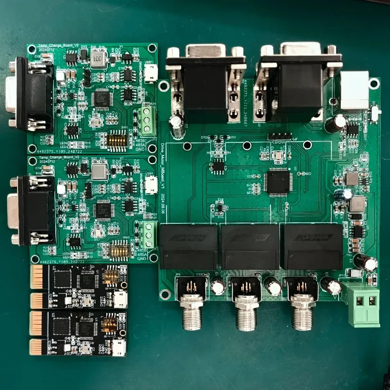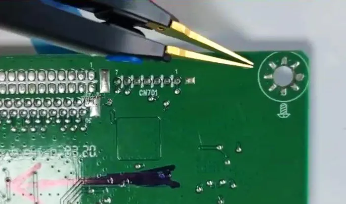
The miniaturization of microwave equipment has driven the development of microwave circuits toward smaller sizes, high integration, high reliability, low power consumption, and mass production.
Microwave PCB Technology and Vacuum Eutectic Soldering for High-Reliability Assembly
The dimensions of microwave devices in microwave integrated circuits (MICs) and monolithic microwave integrated circuits (MMICs) have been significantly reduced, and microwave circuits have also become planar.
PCB as the Core Interconnection Medium
Printed circuit board (PCB) manufacturing processes are characterized by large-scale, high-volume production and low cost;
Consequently, PCBs are the most widely used medium for the mounting and interconnection of MICs and MMICs.
The conductors on microwave PCBs serve not only as interconnections between microwave components but also as microwave transmission lines, performing functions such as phase matching, impedance matching, and balanced transitions.
High-Frequency Substrates and ROGERS Materials
The dielectric properties of high-frequency copper-clad laminates directly affect the performance of microwave transmission lines; therefore, high-performance high-frequency copper-clad laminates form the foundation for manufacturing high-performance microwave printed circuit boards.
ROGERS substrates are characterized by a low dielectric constant and superior temperature stability, with a thermal expansion coefficient of the dielectric that closely matches that of copper foil.
Due to their low dielectric loss and the high reliability of metallized vias, they are commonly used in high-frequency microwave circuit boards.
This paper uses printed circuit boards made from ROGERS substrates for soldering research.
Substrate Grounding and Interconnection Requirements
Substrate grounding interconnection technology is one of the key process technologies in the assembly of microwave components.
Especially during the soldering of high-frequency circuit boards, adequate grounding is the foundation for achieving good performance of microwave components.
Soldering Processes for Microwave PCBs
Currently, the soldering methods for printed circuit boards include reflow soldering and vacuum eutectic soldering.
When soldering complex or large-area printed circuit boards, the “masking effect” of solder is prone to occur during the reflow soldering process, leading to serious quality issues such as solder leaks, bridging, and insufficient solder fill.
Eutectic soldering, also known as low-melting-point alloy soldering, is characterized by the ability of two different metals to form an alloy at a temperature far below their respective melting points in specific proportions.
It offers advantages such as high thermal conductivity, low electrical resistance, and high reliability.
The soldering process for printed circuit boards is performed in a vacuum eutectic furnace, where the atmosphere, pressure, and temperature must be controllable to ensure a controlled soldering process and enhance the reliability of ground connections.
Vacuum eutectic furnaces can provide vacuum, reducing, and inert gas environments, effectively preventing solder oxidation during the process and ensuring a bright surface finish at the joints.
Solder porosity is a key indicator affecting joint integrity, and soldering under vacuum conditions can effectively reduce this porosity.
Principles of Vacuum Soldering
Under vacuum or in a protective atmosphere, the solder is heated to its melting point, whereupon it melts and reacts chemically with the metal on the back of the printed circuit board and the substrate surface to form intermetallic compounds, thereby achieving a reliable connection between the printed circuit board and the substrate.
Key Process Factors Affecting Eutectic Soldering Quality
The primary factors affecting the results of eutectic soldering of printed circuit boards include the temperature profile, soldering pressure, and the size of the solder pad.
Optimizing the soldering temperature profile is a key challenge in the eutectic soldering process.
Several factors must be considered simultaneously during PCB soldering: the process involves a relatively rapid heating and cooling cycle, and the number of components being soldered affects heat distribution within the fixture;
For PCBs, temperatures that are too low result in insufficient wetting of the soldering surface, while temperatures that are too high can cause the gold plating on the ground vias to melt away;
The effects of heating and holding times must also be considered—too rapid a heating rate can cause thermal shock and deform the PCB, while excessive heating time can damage the circuit metals;
When setting the temperature profile, the impact of random events must also be considered, such as vacuuming, gas filling, and venting processes.
The flow rates during protective gas filling and venting/cooling must be fully accounted for.
Influence of Brazing Pad Size on Joint Quality
The area of the brazing pad also affects the brazing results.
If the brazing pad is too small, the brazing interface cannot be sufficiently wetted, leading to lack of penetration in the brazed area and the inability to form rounded edges on component edges, thereby affecting the bond strength between the PCB and the substrate.
Brazing Pressure and Filling Mechanism
Brazing pressure: During the brazing process, the filling length L of the molten brazing material in the brazing joint can be expressed as:
L=2σcosθ/hρg (1)
In the equation, σ, θ, h, ρ, and g represent the surface tension of the molten solder, the contact angle, the gap between the printed circuit board and the substrate, the density of the solder, and the acceleration due to gravity, respectively.
Applying additional weight to the surface of the printed circuit board—that is, reducing the value of h—is an effective method for increasing the length of the gap filled by the liquid solder.
The magnitude of the pressure is achieved through the self-weight of the pressure mold fixture, but the pressure value must be strictly controlled: if the pressure is too low, air bubbles cannot be effectively removed from the solder joint;
If the pressure is too high, it may cause damage to the circuit patterns on the PCB surface.
Reflow Soldering and Eutectic Soldering Tests
This study primarily investigates the effects of two different soldering methods—reflow soldering and vacuum eutectic soldering—on the solder joint quality between ROGERS-5880 printed circuit boards and gold-plated enclosures.
Test Procedure
1. Pre-welding Cleaning
Prior to welding, subject the cavity to be welded and the soldering surfaces of the printed circuit board to plasma cleaning for 9 minutes to effectively remove harmful contaminants such as oxide layers and metal ions from the soldering surfaces.
Plasma cleaning provides a microscopic-level cleaning that cannot be replaced by mechanical wiping; therefore, it is essential to perform plasma cleaning before welding.
2. Conventional Reflow Soldering and Eutectic Soldering Tests
Conventional reflow soldering was performed using tin-silver-copper (SAC305) solder strips (coated with flux) to solder cleaned soldering chambers and printed circuit boards from the same batch.
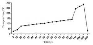
The reflow soldering temperature profile is shown in Figure 1 and consists of four stages: preheating, heating, melting, and cooling.
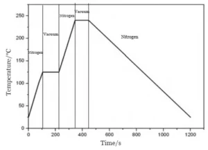
The temperature curve for vacuum eutectic soldering is shown in Figure 2.
The vacuum soldering process for printed circuit boards is reflected in the soldering process curve, which includes temperature and vacuum levels.
The temperature curve can be divided into four stages: preheating and holding (vacuum extraction), heating, solder melting and holding (vacuum extraction), and cooling.
The organic components in the flux volatilize when heated during the preheating stage (at a bench temperature of 125 °C).
After holding for 2 minutes while evacuating the chamber, the organic volatiles are removed, reducing the “masking effect” of the solder.
Proper control of the preheating temperature can prevent cold solder joints, warping, and deformation of the printed circuit board.
The primary influencing factors during the soldering stage are the solder melting temperature and soldering time.
For tin-silver-copper eutectic solder, generally speaking, higher temperatures improve solder wettability;
However, excessively high soldering temperatures can adversely affect the performance of the microwave transmission line.
Based on soldering guidelines provided in the literature, the soldering temperature is set at 235–240 °C, with a soldering time of 2 minutes.
During the soldering stage—specifically after the solder has completely melted—a vacuum must be maintained to remove residual gases from the underside of the printed circuit board and reduce the incidence of solder voids.
Analysis of Test Results
SnAgCu solder pads were used to solder the ROGERS-5880 printed circuit board for the X-band low-noise amplifier (LNA) baseplate.
The soldering methods employed were reflow soldering, eutectic soldering, and vacuum eutectic soldering.
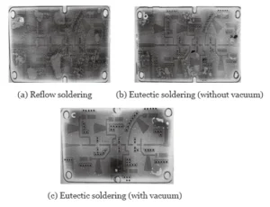
Figure 3 shows X-ray non-destructive testing images of the samples after soldering.
The test results indicate that the reflow-soldered PCB samples exhibit significant voids, and the number of voids is high.
Although the heating rate was strictly controlled during the process, it is difficult to ensure uniform heating of the soldered components due to the large chamber volume of the reflow oven.
Additionally, no nitrogen shielding was employed during the reflow soldering process.
This made the solder highly susceptible to oxidation during melting, resulting in an increased contact angle and reduced solder flowability.
Furthermore, the organic solvent gases released by the flux were unable to escape easily; upon cooling, these gases became trapped within the solder, leading to a high number of voids.
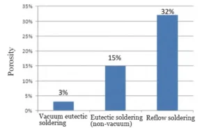
The calculated void rate was approximately 32%, which fails to meet the requirements for high-frequency or military-grade microwave components.
The eutectic furnace chamber is smaller, and nitrogen is introduced for atmosphere protection during the soldering process.
Although the solder is not evacuated during melting, significant voids still appear on the underside of the printed circuit board, with a calculated void rate of approximately 15%.
Eutectic soldering followed by an appropriate vacuum holding process results in a significant reduction in the void rate of the post-soldering samples, with a void rate of approximately 3%, yielding the best soldering results.
Figure 4 shows the calculated void rate.
Eutectic Soldering Tests of Sn-Pb and SnAgCu Solder Sheets
With the trend toward lead-free soldering materials, significant process adjustments are required to meet the demands of lead-free soldering.
Among current lead-free solder alloys, the SnAgCu series is widely recognized as the most promising alternative to lead-containing solders due to its superior wetting properties and mechanical performance.
SnAgCu-based solder alloys have a melting point of approximately 217 °C, exhibit good ductility, and produce a bright finish.
Since Sn-Ag alloys readily form intermetallic compounds such as Cu₃Sn and Cu₆Sn₅ phases on a Cu substrate, which weaken the mechanical properties of the joint, adding Cu to the Sn-Ag alloy can reduce Cu diffusion into the solder and improve wettability.
This also enhances strength and refines the microstructure; however, excessive addition can lead to an increase in the melting point.
Introduction to the Test Procedure
The two types of cut solder foils were simultaneously subjected to plasma cleaning for 9 minutes to remove surface oxides.
Using Sn-Pb and SnAgCu solder pads, respectively, solder the spacers from the same batch to ROGERS-5880 printed circuit boards (50 Ω traces) via eutectic soldering.
During the eutectic soldering process, vacuum and non-vacuum treatments were applied during the solder melting stage, as shown in Table 1.
表1
Analysis of Test Results
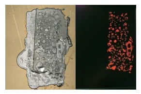
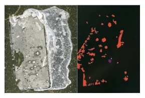
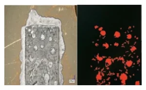
Figures 5 and 6 show photographs of welded samples and void fraction test results for Sn-Pb alloy sheets during eutectic brazing, both with and without vacuum evacuation.
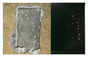
Figures 7 and 8 show photographs of welded samples and void fraction test results for SnAgCu alloy sheets during eutectic brazing, both with and without vacuum evacuation.
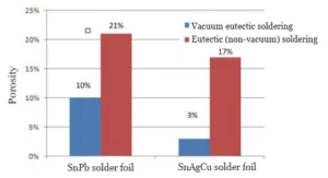
Figure 9 shows the calculated void rates for the samples. The void rates of the samples from the eutectic soldering process with vacuum evacuation were significantly lower than those of the samples without vacuum evacuation.
The samples from the vacuum eutectic soldering of Sn-Ag-Cu pads exhibited the lowest void rates and the smoothest soldered surfaces, indicating that these process parameters are suitable for soldering Sn-Ag-Cu pads.
Currently, the vacuum eutectic brazing process for SnAgCu brazing sheets has been successfully applied in the brazing of printed circuit boards for various microwave components at our organization.
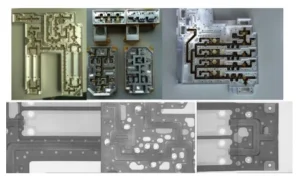
As shown in Figure 10, X-ray inspection images reveal minimal porosity in the brazed printed circuit boards, with smooth brazing surfaces and excellent electrical contact.
Conclusion
This paper investigates the soldering of ROGERS-5880 printed circuit boards using SnAgCu solder foils, comparing reflow soldering and vacuum eutectic soldering processes.
The results indicate that the vacuum eutectic soldering process significantly reduces solder voids, with a void rate of less than 3%, demonstrating a clear advantage over the reflow soldering process.
By controlling appropriate process parameters such as preheating parameters, soldering temperature, and hold time, and by using soldering fixtures with suitable pressure, the soldering quality of lead-free SnAgCu solder foils in vacuum eutectic grounding applications is highly reliable.